Stacking layers of two-dimensional materials on top of each other and varying the twist angle between them massively alters their electronic properties. The trick is to get the twist angle just right, and to know when you’ve done so. Researchers in China have now developed a technique that helps with the second part of this challenge. By allowing scientists to directly visualize the variations in local twist angles, the new technique shed light on the electronic structure of twisted materials and accelerate the development of devices that exploit their properties.
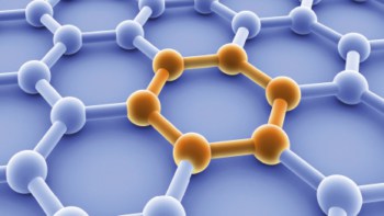
Graphene (a 2D form of carbon just one atom thick) does not have an electronic band gap. Neither does a pair of graphene layers stacked on top of each other. However, if you add another 2D material called hexagonal boron nitride (hBN) to the stack, a band gap emerges. This is because the lattice constant of hBN – a measure of how its atoms are arranged – is nearly the same as that of graphene, but not exactly. The slightly mismatched layers of graphene and hBN form a larger structure known as a moiré superlattice, and the interactions between nearby atoms in this superlattice allow a gap to form. If the layers are then twisted so that they are further misaligned, the lattice interactions weaken, and the band gap disappears.
Achieving such changes in conventional materials usually requires scientists to alter the materials’ chemical composition. Varying the twist angle between layers of a 2D material is an entirely different approach, and the associated possibilities kickstarted a new field of device engineering known as twistronics. The problem is that twist angles are hard to control, and if different areas of a sample contain unevenly distributed twisted angles, the sample’s electronic properties will vary from location to location. This is far from ideal for high-performance devices, so researchers have been exploring ways to visualize such inhomogeneities more precisely.
A new method based on sMIM
In the new work, a team led by Hong-Jun Gao and Shiyu Zhu of the Institute of Physics, Chinese Academy of Sciences, adapted a method called scanning microwave impedance microscopy (sMIM) that was recently developed by Zhixun Shen and colleagues at Stanford University in the US. The adapted method involves applying a range of gate voltages to the sample and analysing conductivity fluctuations in the sMIM data at different positions in it. “This process provides the gate voltages corresponding to moiré band gaps, which are indicative of fully filled electronic bands, directly unveiling details about the moiré superlattice and local twist angles,” Zhu explains.
When the researchers tested this method on high-quality samples of twisted bilayer graphene fabricated by their colleagues Qianying Hu, Yang Xu and Jiawei Hu, they were able to detect variations of twist angles directly. They also gleaned information on the conductivity of localized areas, and they characterized other electronic states such as quantum Hall states and Chern insulators by applying out-of-plane magnetic fields. “We made these measurements concurrently,” Zhu notes. “This allowed us to directly obtain quantum state information under different local twist angle conditions.”
The new technique revealed pronounced variations in the local twist angles of around 0.3° over distances of several microns, he adds. It also enabled the team to measure local conductivity, which is not possible with alternative methods that use single-electron transistors to measure compressibility or nanoSQUIDs to measure magnetic fields. What is more, for samples of twisted bilayer graphene covered by an insulating BN layer, the new method has a significant advantage over conventional scanning tunnelling microscopy, as it can penetrate the insulating layer.
Exploring novel quantum states
“Our work has revealed the local twist angle variation within and between domains of a twisted two-dimensional material,” Zhu tells Physics World. “This has deepened our understanding of the microscopic state of the sample, allowing us to explain many experimental phenomena previously observed in ‘bulk-averaging’ measurements. It also provides a way to explore novel quantum states that are difficult to observe macroscopically, offering insights from a microscopic perspective.”
Graphene ribbons advance twistronics
Thanks to these measurements, the unevenness of local twist angles in twisted two-dimensional materials should no longer be a hindrance to the study of novel quantum states, he adds. “Instead, thanks to the rich distribution of local twist angles we have observed, it should now be possible to simultaneously compare various quantum states under multiple local twist angle conditions and band structure conditions in a single sample.”
The researchers now aim to extend their technique to a wider range of twisted systems and heterostructure moiré systems – for example, in materials like twisted bilayer MoTe2 and WSe2/WS2. They would also like to conduct bulk-averaging measurements and compare these results with local measurements using their new method.