Many researchers around the world are investigating new techniques to reduce the size of integrated circuits. A breakthrough by Joseph Thywissen and Mara Prentiss at Harvard University in the US shows the potential of one such technique, which uses atoms rather than light to carve the features in chips. They have demonstrated that the resolution of "atom lithography" need not be limited by the wavelength of light (arXiv.org/abs/physics/0209084).
Chip manufacturers currently make integrated circuits by shining light through a stencil or “mask” of the circuit design, passing this light through a series of lenses to reduce the size of the image, and then projecting this image onto a silicon substrate covered by a photosensitive resist. Chemicals are then used to wash away the exposed areas of the resist, leaving just the pattern of the mask on the silicon. However, the lenses do not work at short wavelengths and consequently limit the minimum feature size to about 100 nm.
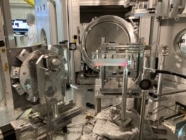
Thywissen and Prentiss have overcome this problem in principle by exposing a silicon substrate to a beam of “metastable” argon atoms. These metastable atoms exist in a naturally excited state and release their energy when they strike the substrate. A layer of hydrocarbons that resides on the substrate functions as the resist by adhering more strongly to the substrate when energized.
To create a pattern in the atom beam, the researchers used a mask made of laser light. The argon atoms resonant with the light are excited into an even higher state, but they fall back down to the ground state almost instantaneously, depriving the resist of energy at the points below the mask.
In previous experiments, this mask was created by forming a standing wave from a resonant laser beam. Only atoms that passed through points of minimum intensity on the standing wave reached the resist in a metastable state. However, the resolution of this approach is fundamentally limited because the undulations in such a standing wave are equal to half the wavelength of the light.
In the latest work, the mask consists of two overlapping laser beams, one of which is made up of a number of discrete frequency components that approximately match the excitation energy of the argon atoms. The other laser beam creates a potential gradient across the atom beam, shifting the atoms into resonance at particular points in space. At these points the atoms fall to the ground state, leaving the resist unstrengthened.
“By modifying the frequency rather than the intensity of the light, the resolution of the mask is not limited by optical diffraction,” says Thywissen. “This is similar to magnetic resonance imaging, which can produce images whose resolution is much smaller than wavelength of radiation used.”
Thywissen and Prentiss’ technique produced features with a minimum width of about 900 nm, still two orders of magnitude larger than the smallest so far achieved using atom lithography. However, since the new technique is not diffraction limited, it could in the future generate smaller features than other atom-based systems.
“Atom lithography has long demonstrated feature sizes smaller than the diffraction limit of light,” says Thywissen. “What is new in our research is that the spacing between the features can also be much smaller, even when using light to do all the patterning.” He says that demonstrating this potential will require more laser power and a more finely collimated atomic beam.