Researchers in Japan have for the first time propagated infrared light through an optical crystal film grown on a silicon substrate. According to the team, the breakthrough could pave the way for more compact communications devices that perform both electrical and optical processing functions on a single chip.
Current optical communications systems exploit silicon-based integrated circuits for processing electronic signals, and separate devices for processing optical signals. For optical switches and modulators to be created on a silicon substrate, a material with a strong electro-optical effect (where the refractive index changes under an applied voltage) must be formed on the substrate.
One suitable material is the ferroelectric material lead zirconate titanate (PZT). But it has so far been difficult to propagate light successfully through PZT, due to disruption of its crystal structure caused when a single-crystal film is formed on top of the silicon substrate.
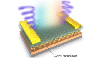
Now a team of engineers from the Tokyo Institute of Technology and Fujitsu laboratories have overcome this problem by fabricating a three-layer buffer between the PZT optical layer and the silicon base. The buffer minimizes disruption to the film’s atomic alignment, as well as preventing any reaction between the optical layer and the silicon substrate.
The buffer zone comprises strontium ruthenium oxide, ceria, and yttrium-stabilized zirconia layers, over which a single-crystal film of PZT is formed.
Using the standard wavelength of infrared light used in optical communications, 1550 nm, the PZT propagation loss was reduced to less than 1 decibel per centimetre. This is claimed to be only 10% of the losses usually seen in PZT.
This work brings closer the ultimate goal of processing both electrical and optical signals on a shared substrate, removing one of the major barriers to any substantial integration and opening up the prospect of ultra-compact optical communications systems.
The new technology was supported by the Japanese government, and will be presented at the 24th Meeting on Ferroelectric Materials and Their Applications (FMA-24) and at the International Symposium on the Application of Ferroelectrics (ISAF 2007) to be held in Nara, Japan, from 27 May 2007.


