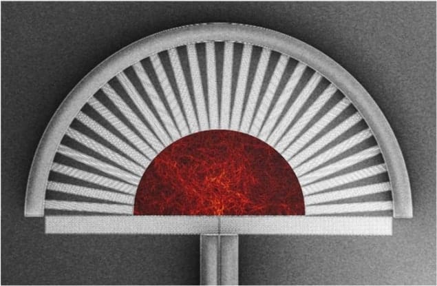
The disordered scattering of light in a special silicon crystal has been used to make a tiny “spectrometer on a chip”. According to its creators at Yale University in the US, the device can measure the wavelength of light with nanometre-scale resolution and is just microns in size. The team believes that the new technology could lead to the integration of spectrometers into lab-on-a-chip systems.
The lab-on-a-chip is a well-established concept that involves using silicon fabrication techniques to miniaturize and integrate analytical processes that are normally performed in a chemistry or medical laboratory. The benefits are most obvious in medicine, where these portable devices can deliver rapid diagnoses that would have previously required sending a sample to an external facility for analysis. Labs-on-a-chip can also be useful research tools, allowing for the rapid screening of candidate drug compounds for effectiveness and toxicity, for example.
Difficult to miniaturize
Spectroscopy is one of the key tools of analytical chemistry. It involves identifying a material using the specific set of light wavelengths that it emits, absorbs, reflects or transmits. Traditional spectrometers use a diffraction grating to spread the wavelengths out at slightly different angles so that the spectrum can be obtained using a position-sensitive detector. This is inherently difficult to miniaturize because the angular resolution and therefore the wavelength resolution of the instrument depends on how far the light travels after passing though the diffraction grating. The smaller you make the spectrometer, therefore, the less sensitive it becomes.
Several groups have designed spectrometers that evade this constraint by, for example, using resonant cavities to increase the optical path length beyond the physical size of the device. Other attempts rely on using different physical principles, such as the wavelength-dependent interaction of light with photonic crystals. These have had some success but they all have limitations, including manufacturing difficulties, low sensitivities or inability to deal with broadband spectra.
Highly nonlinear path
In the new research, physicists at Yale have produced a spectrometer that identifies the different wavelengths present by shining light into a semi-circular crystal of silicon studded with tiny holes. The light scatters repeatedly off the holes, travelling a complex, highly nonlinear path – much longer than the physical dimensions of the crystal – between entering the crystal and leaving at the outer edge. An array of waveguides attached to the outer edge delivers the light to a series of photodetectors, allowing the light intensity arriving at closely spaced points to be measured.
In general, the movement of light within the silicon crystal is effectively random and therefore so is the intensity distribution produced. However, the researchers verified that putting in the same wavelength always produced the same distribution and that when they changed the input by only a small amount the pattern changed only gradually. “There’s a correlation wavelength you can think of,” explains Yale’s Brandon Redding, “which is the change in wavelength you need before the intensity pattern changes noticeably. And so within that, different wavelengths produce pretty much the same pattern.” For larger differences in wavelength, the patterns produced by various wavelengths are effectively independent.
Catalogue of patterns
The team calibrated the spectrometer by looking at the intensity pattern at a series of known wavelengths separated by about this correlation width. Cataloguing the patterns produced by all wavelengths of interest allowed the researchers to calculate the wavelengths present in an arbitrary beam of light. To demonstrate this, they constructed a spectrometer with a radius of just 25 μm and calibrated it for wavelengths of 1500–1525 nm. They found that they could resolve spectral lines just 0.75 nm apart or accurately reconstruct a broadband spectrum of these wavelengths.
Allard Mosk, an expert in complex photonic systems at the MESA+ Institute for Nanotechnology of the University of Twente in the Netherlands, describes the work as “excellent”. “The present device does not significantly exceed the resolution, throughput or other specs of any existing device as yet,” he says, but adds that the technology shows great promise. He concludes, “I expect this result to give rise to the development of devices optimized with specific application areas in mind, as well as highly optimized devices that may exceed, for example, the spectral resolution of devices with a similar footprint.”
The Yale team leader Hui Cao also hopes that the idea will be developed commercially outside the research lab. “We are applied physicists,” she says, “We try to develop a novel device concept using a physics principle. We are hoping that somebody will take this over and try to develop it into a commercial product and we will be very happy to help.”
The research is described in Nature Photonics 10.1038/nphoton.2013.190.


