Jon Major assesses how the materials used to make solar photovoltaic cells have evolved from first-generation silicon up through thin films, perovskites and (maybe) beyond

Ten years ago, solar photovoltaic (PV) power generation was something of a curiosity. The entire world boasted only about 10 gigawatts of generation capacity, over 40% of which was in Germany, and these early installations were typically supported with generous government subsidies. A decade of phenomenal growth has changed this picture utterly. In 2018 the world’s installed capacity will likely surpass 500 GW – enough to power the whole of Brazil.
This astonishing and near-exponential growth has, for the most part, been driven by simple economics. Just as automobiles only really started to replace horse-drawn vehicles following the advent of the mass-market, affordable Model T Ford, solar’s upswing accelerated when prices entered the realm of cost-competitiveness with fossil fuels. Initially, near-parity came with the help of subsidies, but at some point – the exact moment is hard to pin down, as the costing is complex – most reliable information sources began to show that even without them, cost-parity with fossil fuels is now within reach.
This achievement is all the more remarkable because it has happened without any dramatic shift in the underlying PV technology. In the main, today’s solar cells are very similar to the one demonstrated at Bell Laboratories in 1954. That device – the first true solar cell – was based on a simple junction between n-type (electron-rich) and p-type (electron-poor) silicon, and it converted sunlight into electricity with an efficiency of 5%. Over the years, increasing sophistication in cell design, via the addition of highly doped silicon and anti-reflection layers, has pushed the efficiency to over 25%, but the core p-n junction structure remains. As a result, even though silicon PV is rapidly approaching pensionable age, when it should be putting up its feet and letting younger whippersnapper technologies carry the load, it still accounts for around 95% of the global solar market.
Given its status as the leading solar-cell technology, [silicon] has a slightly unfortunate characteristic: it doesn’t absorb light very well.
The question is, does it matter? After all, silicon PV works. Its price has come down to a competitive level. Where is the problem? As with most semiconductor-related matters, the answer lies in the core properties of the material. Silicon is undoubtedly the world’s favourite semiconductor, underpinning most of modern computing amongst myriad other applications. However, given its status as the leading solar-cell technology, it has a slightly unfortunate characteristic: it doesn’t absorb light very well.
The light-absorption properties of semiconductors depend on the energy separation between their conduction and valence bands of electrons. Such bandgaps fall into two types: direct-gap and indirect-gap. For indirect-gap materials, of which silicon is one, the process of absorbing an electron is phonon-assisted due to the presence of an offset in the respective minima and maxima of the band structure. While this may sound like a minor problem, it means that indirect materials absorb light much less strongly (the difference is several orders of magnitude) than their direct-bandgap cousins, which require no phonon assistance.
This basic material property in turn defines the practicalities of producing silicon solar cells. Because silicon absorbs light relatively weakly, greater thicknesses of material are required to ensure that sufficient light is absorbed. The total thickness is generally only hundreds of microns, and for you and me, that might seem trivial. For an electron, though, with a considerably shorter stride length, it’s a significant distance to travel. Hence, for electrons to traverse the material effectively, PV-grade silicon must take the form of highly crystalline, high-purity wafers.

This means one thing: cost. Silicon production for solar modules is a large-scale, complex and surprisingly slow wafer-growth process. Were it not for the material’s links to the microelectronics industry (and related economies of scale from mass production in East Asia) the cost of silicon PV would never have fallen as low as it has, and if the price of solar power production continues to fall, the material production costs will at some point become a limiting factor.
Looking beyond silicon
The drive to cut production costs is one reason why research in the field has long focused on alternative materials. If silicon is the solar equivalent of cathode-ray tube – something that does the job but is rather antiquated and a bit chunky – then the time will come when everyone will want to transition to a nice flat-screen, ultra-high definition version. Fortunately, a second generation of PV technology is already well established in the form of thin-film solar cells. In particular, two materials, cadmium telluride (CdTe) and copper indium gallium selenide (CuIn1–xGaxSe2, or CIGS for short), make highly effective cells. Unlike silicon, they have a direct bandgap, so they need to be only a few microns thick to have sufficient optical absorption (hence the term thin-film). Lower-quality, lower-purity materials are acceptable, and production can occur via rapid deposition methods such as evaporation or sputtering directly onto a piece of low-grade window glass.
Another advantage is that whereas production of the core material for silicon modules is separate from module fabrication, thin-film modules are produced in-line. That means a rolling production process where glass goes in at one end and near-complete modules come out at the other – significantly faster and more streamlined.
These thin-film technologies are not particularly new, being children of the 1970s, but over the intervening decades their performance has gradually improved, tracing the similarly gradual increase in our understanding of how such materials function. It is only relatively recently that their performance has begun to equal that of their flabbier silicon predecessor. Now that this point has been reached, their potential benefits are starting to be realized. Panels are being produced in a fraction of the time, using less starting material, with a lower carbon cost of fabrication, and in a such way that makes them much lighter and sometimes even flexible. This is already a mature industrial technology: companies such as CdTe module producer First Solar have installed gigawatts worth of modules already.
The transition beyond silicon is unlikely to stop with these early thin-film materials, though. The solar research community continues to seek ways to evolve onto the next generation of the technology. A number of third-generation concepts using novel materials physics have been suggested, including “intermediate-band” solar cells, nanostructured devices and hot carrier solar cells. While undoubtedly exciting, practicality has so far not matched prediction in these more radical departures from the established architecture. Instead, a sizeable fraction of research has focused on finding improved thin-film materials.
Any of the current raft of new materials may take off, or all may ultimately fade along with other former great hopes.
One reason that improvements are needed is that although both cadmium telluride and CIGS are highly effective, they rely on tellurium and indium – two of the rarest elements in the Earth’s crust. As we (hopefully) look towards a glorious future of terawatt-level PV power generation, the availability of raw materials will become intrinsically linked to the cost of commercial devices, and thus just as important as the materials’ functionality. This insight has driven interest in what are termed Earth-abundant absorber materials, but progress in developing such materials has often been slow and interest tends to tail off whenever the development process hits a seemingly insurmountable barrier. Although research on new materials has been ever-present, in the early part of this decade there was nevertheless a developing sense in some circles that no improved materials would be found, and that emphasis should therefore be placed on enhancing established technologies.
Promising perovskites
This viewpoint has emphatically changed in recent years with the advent of perovskite solar cells and, in particular, cells based on a compound called methyl ammonium lead iodide (MAPI). This hybrid between organic and inorganic materials first appeared as an off-shoot from the field of dye-sensitized solar cells, where the light-absorbing medium consists of nanoparticles coated with photo-conductive dyes. While various new potential PV materials have appeared over the years, nothing else has had the seismic impact of MAPI. Most technologies have a long development period, with light-to-power conversion efficiencies slowly creeping up over years (and even decades) of research – something that can be seen on the US National Renewable Energy Laboratory’s regularly updated solar-cell efficiency chart (PDF). CdTe and CIGS solar cells, for example, both took around 40 years to reach a conversion efficiency of 20%. The excitement surrounding MAPI stems from the fact that it achieved the same feat in around four years, going from basically unknown to competitive with the highest-efficiency materials out there in a comparative blink of an eye. This caused tremendous excitement in the solar-energy community and research into the material subsequently exploded, with thousands of research papers on MAPI published annually.
Bright starts, fading finishes
Scientists have studied a wide palette of materials for solar cell applications over the years. Far too often, though, progress follows a familiar pattern: someone makes an initial device, interest grows, more cell work follows, problems emerge, the problems can’t be solved, people give up and then move on. The reasons why a given material fails to make the cut tend to be particular to the material itself, and unfortunately, they often only become apparent after a lot of work has been put in.
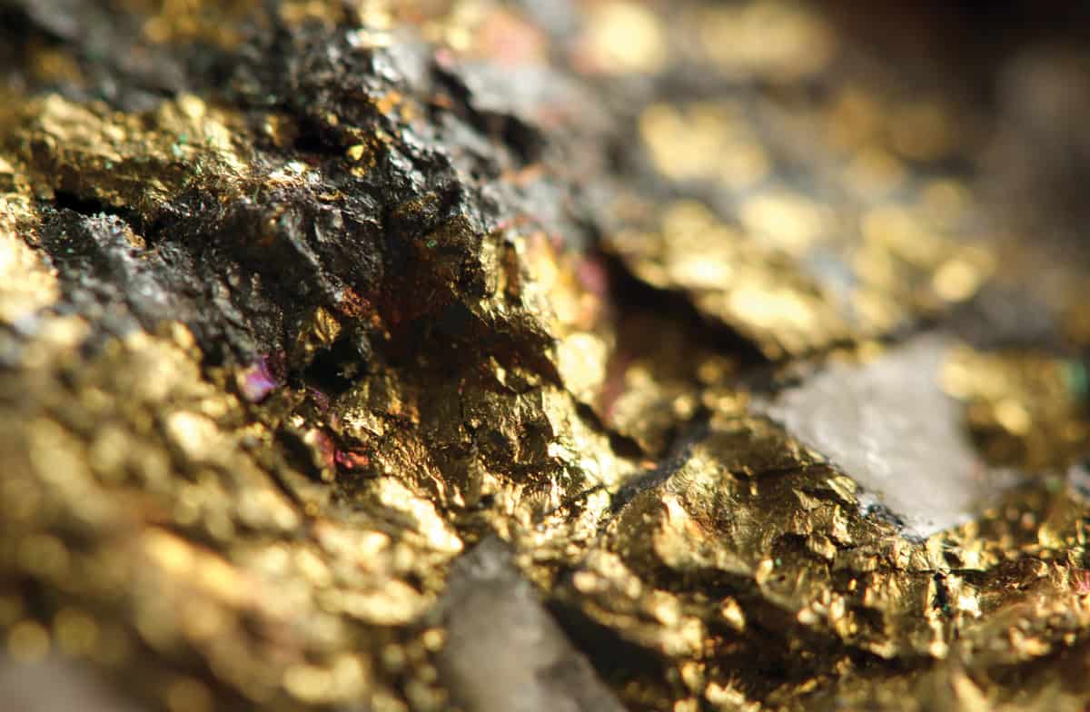
One notable entry on the long list of next big things that never quite panned out is iron pyrite, FeS2. Boasting fantastic absorption properties, a simple structure and a lovely, Earth-abundant composition, it received a great deal of attention in the 1980s and 1990s. Low-efficiency cells were made, but somehow they never really got much better. This was primarily due to problems with the surface of the material, which behaves in a way that is dramatically different to the rest of it; in fact, it remains an open question whether films of the material are n-type or p-type. The fact that pyrite is commonly known as fool’s gold is entirely coincidental.
Other earth-abundant materials have had similar struggles. PV cells made from tin sulfide have reached similar performance levels as pyrite. However, moving beyond that mark has been a struggle, since tin sulfide takes on many different phases depending on how it is produced, and this changes the doping completely. Theorists predicted that copper bismuth sulfide would be a wonder material, but it proved tremendously tricky to work with, as the precursor material would much rather form copper sulfide and bismuth sulfide separately. Consequently, even the best cells made from copper bismuth sulfide barely produce a current. An amorphous, non-crystalline, version of silicon also attracted considerable research interest after it was found to have an increased bandgap and higher optical absorption, allowing it to be used as a thin film. Unfortunately, the down side of its amorphous nature was an inherently large number of defects in the material. Despite a vast amount of research, the efficiency of amorphous silicon solar cells has never exceeded ~11%, with the high defect density forming an apparently insurmountable limit. These materials may ultimately be resurgent, but for the moment they serve as an example of how hidden issues can scupper the development of new solar-cell materials.
However, for all its wonderful properties, MAPI also turned out to have limitations. As well as converting sunlight efficiently and being relatively inexpensive, PV materials must also be highly stable. This is because there are additional costs, beyond those of the actual solar cell, associated with setting up a module array. These balance of systems costs mean that for a PV technology to be economically viable, cells must survive use for decades. Unfortunately, MAPI degrades rapidly when exposed to moisture and sunlight – clearly less than ideal for a material intended to be placed on a rooftop. These stability issues are by no means the death knell of the material, as they may yet be solved, but MAPI is looking a little less like the ultimate solution than it once did.
Playing the numbers
What MAPI’s emergence has done, though, is to showcase once more the potential of new materials for PV. If something like MAPI can appear from nowhere and develop at such a blistering pace, it raises the tantalizing prospect that other such materials may exist, but have yet to be tested. The overall impression is that we are entering an age of accelerated materials discovery, encompassing both experiment and theory. Rapid material-screening methods have become increasingly sophisticated, with numerous research groups able to deposit and characterize the properties of a new PV material, at a range of compositions, in a single step. This makes it possible to create material-property libraries in a fraction of the time required previously.
This work is underpinned by specialists in density functional theory, who use supercomputer-based calculations to predict the band structure, defect composition and stability of new compounds – all of which helps guide experimentalists. Emerging early-stage cell technologies are receiving renewed interest; the MAPI research community has now mutated into a broader research area focused on perovskite structured devices; and inorganic nano-ribbon compounds such as antimony selenide are showing early signs of promise.
All of this research is something of a numbers game. Any of the current raft of new materials may take off, or all may ultimately fade along with other former great hopes. Without a solar-powered crystal ball, it is hard to say which materials will persevere. The silicon standard-bearer may continue to dominate thanks to its industrial might; established thin-film materials may continue to grow market share; or an unheard-of new material may rise above the crowd thanks to the recent surge in materials discovery.
It also seems plausible that numerous complimentary solar technologies will enter a sort of symbiotic co-existence, with different materials finding different applications. Silicon, for example, might remain dominant for rigid modules, whereas thin-film may become the go-to choice for integrating power generation into buildings or providing lightweight power generation in remote areas. Other newer, still undeveloped, technologies may become the solution to an as-yet-unrealized need. Whatever happens, the palate of useable PV technologies is being continually broadened in tandem with falling prices. The dream of parity with fossil fuels has been reached by quiet and gradual evolution, but a material revolution may yet be a true game changer.
- Enjoy the rest of the 2018 Physics World Focus on Energy Technologies in our digital magazine or via the Physics World app for any iOS or Android smartphone or tablet.