
High-resolution imaging shows how oxide layers modify graphene’s electrical behaviour

Graphene, an atomically thin material of a single layer of carbon atoms, is a fascinating material for high-speed electronics, spintronic devices, and neuromorphic components due to its exceptional tunable electrical conductivity. One area of research focuses on understanding how electrons flow through graphene to enable the design of advanced devices. For applications, ultrathin metal-oxide layers (e.g., aluminum oxide and titanium oxide) are routinely deposited on graphene, which deliberately alter electron flow and provide greater control over its properties, in devices ranging from transistors to spin valves. However, although the effects of these coatings are known, researchers have not previously been able to directly observe what is happening inside the device. Instead, their understanding has relied primarily on theoretical models, numerical simulations, and indirect electrical measurements.
In this work, the researchers used X-ray Photoelectron Spectroscopy (XPS) to map electrical potentials across devices while they were operating. They examined the electrical landscape, identifying regions with steep slopes corresponding to strong electric fields and flatter regions corresponding to weaker electric fields, to determine how oxide coatings modify this landscape. They found that metal oxides flatten the electrical landscape through a process known as p-type charge-transfer doping. This occurs when the oxide removes some electrons from the graphene, altering its local electrostatic environment and reducing the voltage gradient. As a result, local electric fields become weaker. The oxide layers suppress the electric fields, reducing them by more than 50%, a significant effect for device operation. A key advance of this research is the visualisation of this effect at very high spatial resolution, whereas previously it could only be inferred from electrical resistance measurements. In addition, by making a direct comparison with electrical measurements, the researchers confirmed the observed effects are due solely to electrostatics and charge redistribution.
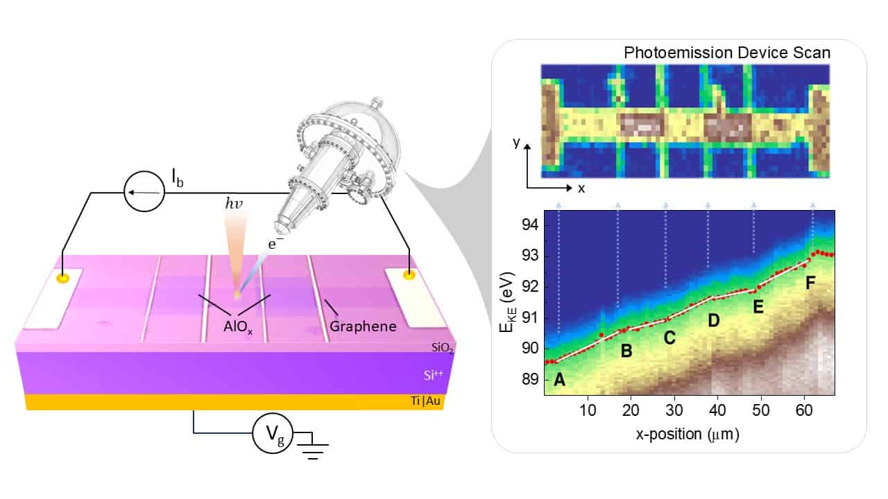
Modern electronic devices increasingly depend on controlling electricity at very small scales. By locally adjusting electric fields using oxide coatings, researchers gain an additional design tool that enables different regions of a graphene circuit to be tuned independently. This is particularly important for spintronic devices, which are highly sensitive to local electric fields, and neuromorphic computing hardware, which requires precise control of local electrical properties.
This work represents a breakthrough in the ability to directly map charge distributions and electric fields inside operating 2D-material devices, enabling improved device design.
Read the full article
Umidakhon Rayimjonova et al 2026 Rep. Prog. Phys. 89 060502
Do you want to learn more about this topic?
Phonons and thermal transport in graphene and graphene-based materials byDenis L Nika and Alexander A Balandin (2017)
