Quasicrystals are unusual yet relatively common materials. They show up in lots of different places from alloys to colloids and even in meteorites. They have some ordered structure, but unlike ordinary crystals their patterns never repeat.
This mix of order and irregularity leads to interesting behaviour when waves move through them. In optical versions of these materials, light can become trapped or guided in ways that doesn’t happen in regular structures.
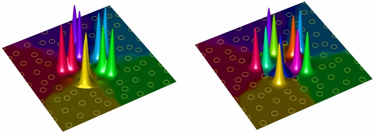
In a new study published recently, a team of researchers investigated what happens when light beams with a twist, called vortex beams, travel through quasicrystals that have been deliberately altered. They began with a classic pattern known as the Penrose tiling and then introduce large scale defects by removing or adding wedge shaped sections. This let the researchers tune the rotational symmetry of the structure and compare how light behaves in each case.
Using a standard model for how light travels through the material, the researchers showed that these modified quasicrystals can support new vortex states. These include two distinct types of vortex solitons, which are twisted beams of light that keep their shape as they travel rather than spreading out.
Usually, these light states require carefully tuned input power and are easily disrupted. What’s different in this case though is they form even with weak input and remain stable under small disturbances. This makes them far more applicable to real-world conditions.
These vortex beams can carry information in the amount of twist they have, providing an extra way to encode data alongside commonly used properties such as intensity or colour. If they remain stable as they travel, they would allow more information to be sent through the same optical system. This could be very useful in optical communication systems, where fast and efficient data transmission is essential.
A new method of stabilizing radioactive molecules could open the door to sensitive searches for physics beyond the Standard Model. The approach, which involves cooling radium-bearing molecules to just above absolute zero, offers a tabletop alternative to experiments that use particle accelerators to look for violations of fundamental symmetries. According to lead researcher Nick Hutzler, a physicist at the California Institute of Technology (Caltech), US, it also shows that university laboratories can safely handle these radioactive materials, paving the way for similar studies at other institutions.
One of the greatest puzzles in physics is the fact that the early universe created more matter than antimatter. For decades, physicists have tried to solve this mystery (and others) by using particle accelerators to search for violations of nuclear symmetry at ever-higher energies. However, molecules that contain heavy radioactive nuclei could also act as super-sensitive sensors for symmetry violations – with the advantage that the equipment required to manipulate them generally fits in a single room, rather than an entire building.
Pear review
The basic idea is this: when electron orbitals overlap with a nucleus, the system’s atomic or molecular energy levels shift by tiny amounts that depend on the nucleus’ size and shape. Variations in nuclear structure due to symmetry-violating effects would therefore produce changes in the electron orbitals, and these changes could be measured with high-precision spectroscopy.
Asymmetric nuclei are ideal for this purpose because their lopsided shape makes small changes easier to detect. Radium, for example, has a pear-shaped nucleus, and radium-containing molecules offer additional advantages because the repulsion and attraction of neighbouring atoms further distorts the electron orbitals.
The downside is that radium is both radioactive and highly reactive, making it dangerous to handle without specialized equipment that is not present in standard university laboratories. It is also only available in extremely small quantities.
Sweet as candy
In the latest study, which is published in Science, physicists at Caltech and chemists at Johns Hopkins University and Michigan State University (all in the US) found a possible way around these obstacles. Their first step was to make radium stable and transportable. For this, they developed a process that resembles candy-making, though they do not recommend eating the results. By “caramelizing” small amounts of radium-226 in a solution of xylitol sweetener, they created a material they could transport in small quantities, keeping radioactivity levels low enough to comply with standard radiation-safety frameworks.
Next, they added their sticky radium “goo” to gold foil; installed it in a copper cryogenic cell; and cooled it to 4K using helium gas. They then used a laser to excite the radium into a chemically reactive state, allowing it to bond with targets such as hydroxide, deuteroxide and fluoride. Collisions with surrounding helium atoms further cooled these radium-bearing molecules into a mixture of only a few rotational and vibrational states. At this point, the team was finally able to perform the first-ever high-precision spectroscopic analysis of such molecules.
Opening doors
Hutzler acknowledges that several challenges remain before precision searches for symmetry violation can begin in earnest. Though theory predicts that these radium-bearing molecular species will be amenable to standard laser cooling and trapping techniques, no one has yet cooled them to ultracold temperatures. Another challenge will be to extend the process to other isotopes. Radium-225, for example, has a better nuclear shape for high-precision searches for symmetry violation, but it is also much more radioactive than radium-226, with a half-life of 15 days rather than 1600 years.
The team is also interested in studying the spectra of other radioactive species, with the aim of better understanding nuclear structure and chemistry at the extremes of the periodic table. A final possibility, Hutzler adds, would be to study other radium-containing molecules, as this would enable different precision measurements.
David DeMille, a physicist at Johns Hopkins who studies symmetry violations in atomic and molecular systems but was not involved in this research, calls it an “extremely promising way” to search for interactions that violate charge-parity (CP) symmetry. The efficiency with which the team converts solid-phase radium atoms into gas-phase molecules is a good sign, he adds, and extending the process to other radioactive molecules could help scientists understand species that have been observed astronomically.
However, DeMille points out that achieving ultracold temperatures poses additional challenges, including finding a way to release the confined molecules into a larger, much more complex experimental setup, without helium, while maintaining safe conditions. That said, he notes that the spectroscopic results are, in themselves, an important step towards reaching this ultracold regime.
A new type of “photonic multi-lane highway” that can carry multiple topologically-protected optical signals at once – without the need for a bulky insulator – has been demonstrated by researchers in China. The technology, which relies on a new type of material called a photonic valley half-semimetal to achieve topological protection, is currently at the prototype stage. However, the researchers believe that, if fabrication challenges can be addressed, the combination of spatial efficiency and topological robustness could be promising for future photonic technologies.
In the past 20 years, photonic topological insulators have become widespread for connections in devices such as on-chip photonic circuits because their edge modes can only conduct light in one direction and are therefore are inherently immune from scattering off imperfections. However, the protected edge mode of a topological insulator comes at a cost: the bulk must have an optical band gap, which means it must be opaque to the relevant frequency. Meanwhile, the photonic analogue of another concept from electronics has also become popular in optical waveguides. Gapless photonic semimetals – analogous to graphene – can be placed between topologically distinct optical insulators to broaden the guided modes, but non-guiding insulating claddings are still required.
To address the fundamental trade-off between spatial efficiency and topological protection in conventional topological waveguides, researchers in the group of Che Ting Chan at the Hong Kong University of Science and Technology in China and their collaborators introduced a novel photonic structure called a photonic valley half-semimetal. Here, the valley degree of freedom refers to inequivalent local energy extrema in momentum space, which can be used as independent degrees of freedom for transport. Crucially, a single photonic valley half-semimetal plays a dual role via its two valley channels: one valley acts as a gapless semimetal that enables waveguiding, while the other functions as a topological insulator that provides a topological barrier for the corresponding valley mode in adjacent regions.
Four stacked layers
The researchers designed a waveguide comprising four stacked layers of a honeycomb structure made from interconnected rods of the magnetic material yttrium iron garnet, which interfered with the propagating photons. By altering the diameters of the rods or the magnetic field, the researchers constructed four inequivalent photonic valley half-semimetal domains and arranged them in a specific periodic sequence. This creates adjacent domains that mutually insulate each other.
Xiaohan Cui is lead author on a paper in Nature that describes the research. She explains that the underlying topological physics is similar to that in a traditional photonic topological insulator.
“The important difference lies in how the mode is spatially implemented,” she says, “In a conventional photonic topological-insulator waveguide, two gapped bulk domains meet at an interface, and the propagating mode is tightly localized to that interface. Most of the surrounding insulating material remains inert, serving only as cladding.”
In the present configuration, however, the researchers were able to use the blocked valley as topological protection for unidirectional propagation in the neighbouring domain, and utilize this to create a four-lane highway, with two lanes in each direction, that could guide signals around sharp bends and through constrictions without backscattering or inter-lane crosstalk:
No wasted space
“The architecture transforms the usual narrow interface state into a set of directly adjacent, large-area waveguiding lanes. Consequently, no region of the device is ‘wasted’ as inert cladding,” explains Cui.
The team’s current device works for microwave radiation but the team says that the design could be adapted and extended to operate at higher frequencies.
“The present experiment is a proof of principle demonstration at microwave frequencies, so one clear next step is to move the concept towards higher-frequency, chip-scale integrated photonics platforms, thereby paving the way toward ultra-compact topological photonic circuitry,” says Cui.
The researchers believe application in the terahertz regime should be possible using magnetized semiconductors such as indium antimonide. However, non-reciprocal applications at higher frequencies could be challenging owing to the weakness of magnetic effects.
“The major experimental challenges will be to realize these higher-frequency designs while managing geometric complexity, fabrication tolerances, and propagation loss, and ensuring efficient coupling with practical sources, detectors and other photonic components,” she explains.
Quantum optician Mahmoud Jalali Mehrabad of Massachusetts Institute of Technology believes the work brings an important issue into focus. “A paper doesn’t always have to have the perfect solution as long as it highlights and really streamlines a key problem…To me this paper does that,” he says. “Spatial efficiency has been a problem in topological physics and the question is why? Is there any other way to destroy this trade-off? It shouldn’t be a side problem in the supplementary material of a paper – this is a big problem.” Whether or not the researchers can make their own solution viable, he says, “time will tell”.
A new measurement of the ground-state hyperfine splitting in antihydrogen shows that it is identical to that of normal hydrogen to within four parts per million – two orders of magnitude more precise than previous experiments. Although the measurement by CERN’s ALPHA collaboration did not reveal any asymmetries between matter and antimatter, the result is nevertheless a milestone in the search for reasons why the universe appears to be made up almost entirely of matter, with only minute amounts of antimatter.
According to the Standard Model of particle physics, all matter particles have a corresponding antimatter particle that is identical to them in every way apart from their charge and magnetic properties, which are reversed. If this model is correct, then the Big Bang that formed our universe nearly 14 billion years ago should have generated equal amounts of antimatter and matter. But in that case, neither we nor almost everything else we observe should exist, because pairs of antimatter and matter particles annihilate each other whenever they collide.
“This apparent lack of antimatter in the universe remains one of the biggest mysteries in modern physics and suggests there is something about antimatter and matter that we do not understand,” says Timothy Friesen of the University of Calgary, Canada, one of the lead authors of a Naturepaper on the new measurement.
Measuring antihydrogen
To look for subtle asymmetries that might explain why matter triumphed and antimatter all but disappeared, ALPHA is performing precise measurements on the simplest antimatter atom: antihydrogen, which consists of an antiproton bound to an antielectron, or positron.
These measurements take place at the CERN Antiproton Decelerator Facility using the ALPHA-2 antihydrogen apparatus, which is designed to prevent antihydrogen from coming into contact with normal matter. It does this by confining the antimatter within a cylindrical Penning–Malmberg trap under an extremely high vacuum and surrounded by strong superconducting magnets. These magnets suspend the antimatter in the trap so that it does not touch the walls of the container it is held in, preventing it from annihilating before measurements can take place.
In the latest work, the ALPHA collaboration focused on a parameter known as hyperfine splitting. This splitting occurs because magnetic interactions between the spins of the antiproton and positron cause the positronic ground state in antihydrogen to split into four sublevels, which the researchers label |a⟩, |b⟩, |c⟩ and |d⟩.
In hydrogen, the magnitude of this hyperfine splitting has been measured extremely precisely – we know its value to within a few parts per trillion – and it is particularly sensitive to the structure of the proton. Measuring this splitting in antihydrogen with the same precision would therefore be an excellent way of searching for differences between matter and antimatter. Previously, however, the most sensitive measurements only managed a precision of 400 parts per million (ppm).
In pursuit of precision
To push beyond this level, the ALPHA researchers applied pulses of microwaves at frequencies between 28 GHz and 31 GHz to induce the positron spin flip transitions |c⟩ → |b⟩ and |d⟩ → |a⟩ between the hyperfine levels of ground-state (2S and 1S) antihydrogen atoms. By measuring the frequencies at which these transitions occurred, they could then calculate the hyperfine splitting energy.
“At a magnetic field of 1 Tesla, we measured the hyperfine splitting for antihydrogen to a precision of 4 ppm – a result that has allowed for one of the best comparisons of matter-antimatter symmetry in antihydrogen ever,” Friesen says.
While the new measurement is precise enough to push experiments into a regime that is sensitive to the structure of the antiproton, Friesen notes that it is still five orders of magnitude less precise than comparable measurements in ordinary hydrogen. “The comparisons at this level of precision with matter hydrogen are identical, and our current models of physics therefore still hold,” he says.
The team does have some ideas for further improvements. “To push the measurement to improved precisions we are aiming to induce antiproton spin flip transitions, since these can be less sensitive to magnetic field inhomogeneities, which are our biggest systematic uncertainty,” Friesen explains. “This, combined with laser cooling the antihydrogen samples to reduce the width of our spectroscopic line-shapes, could help improve the precision by at least another factor of 100.”
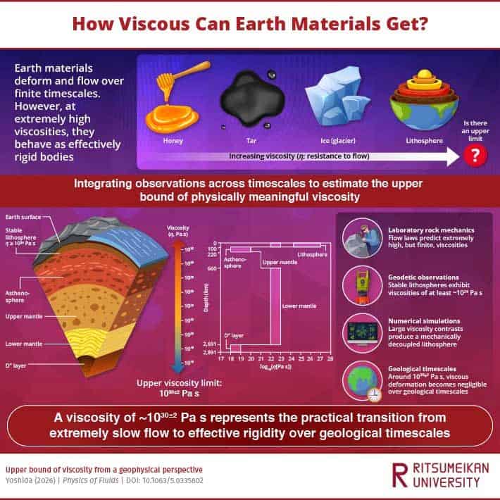
At what point does a material become so viscous that it cannot flow? The question is a tricky one because some apparently solid objects are not as rigid as they seem. A glacier, for example, may look immobile, but when viewed over long-enough timescales, its slow flow becomes apparent.
Now, thanks to satellite observations of tectonic plate deformations as well as physical and geodynamic modelling, geophysicist Masaki Yoshida of Ritsumeikan University, Japan, claims to have found an answer. The upper limit for viscosity, he says, is 1028 Pascal-seconds (Pa s), and the new boundary could yield insights into Earth’s geodynamics.
Viscosity is a measure of a material’s resistance to flow. Gases such as air and hydrogen have a viscosity of 10-5 Pa s at room temperature; the viscosity of liquid water is 10-3 Pa s; and glaciers have a viscosity of 1013–1017 Pa s depending on factors such as temperature, stress and microstructure. At the upper end, Yoshida says that the long-held view, based on rock deformation experiments, is that the viscosity of tectonic plates at the Earth’s surface (where temperatures are relatively low) is 1070 Pa s.
This number is so high that for most purposes, it might as well be infinite, meaning that these plates should behave like rigid bodies. But this accepted wisdom poses a problem: “I realized that I was unable to explain to my students why plates with such high viscosity bend and subduct into the mantle,” Yoshida tells Physics World.
Observed flow and flow parameters
To determine the “effective viscosity” of rock under the temperature and pressure conditions on Earth, Yoshida began by analysing satellite data showing tectonic plate deformations over tens to hundreds of kilometres. Using these data, he could ascertain strain rates – deformations in the plate over a given distance and time – as small as 10-9 per year.
Slow flow: Geodetic observations, laboratory rock-deformation experiments and numerical simulations suggest that there is a geophysically meaningful upper bound of viscosity that marks the transition from deformable flow to effectively rigid behaviour over geological timescales. (Courtesy: Masaki Yoshida/Ritsumeikan University)
By comparing regions under similar stress levels, Yoshida obtained an indication of comparative effective viscosity, which depends on factors such as temperature, composition, grain size, water content, stress state, deformation mechanism and structural heterogeneity. After accounting for assumed stresses, these observations suggested that observed viscosity maxes out at 1028 Pa s.
Yoshida also considered empirical descriptions for the viscosity of various minerals under different types of deformation using parameters from the literature. These yielded a similar upper bound of 1030+/-2 Pa s. Numerical simulations further corroborated this value as a viscosity maximum.
Importance of an upper bound
Taras Gerya, a geodynamicist at ETH Zürich in Switzerland who was not involved in the study, calls Yoshida’s work “an interesting discussion on the significance of viscous deformation for the lithosphere”. However, he notes that, given a realistic stress level of 30 MPa, the maximum viscosity identified gives a cumulative viscous deformation of just 8.5 m for the full 4.5 billion years of Earth’s history. That, he says, is “1000 times smaller than elastic deformation for the same deviatoric stress level”.
While pinning down an exact magnitude for such high viscosities may not greatly change models of deformation, Yoshida thinks that delineating an upper bound may nevertheless improve our understanding of the physical quantities that characterize the behaviour of matter. He also points out that thermal conductivity, which indicates how easily heat is transferred in materials, ranges over only about five orders of magnitude from water to diamond, making it “surprising that viscosity spans a range of about 35 orders of magnitude”.
Yoshida is keen to explore other implications of these results. During the first hundreds of millions of years of Earth’s existence, when it formed and rapidly cooled, he explains that it was covered by a single rigid lid known as the lithosphere. Plate boundaries and motion didn’t emerge until later, approximately 4 billion years ago. “I believe that the question of why plate motion began after the rigid lid formed is closely related to the results of this study,” he says.
Researchers in China have cross-calibrated radiation detectors on 25 navigation satellites. Data from two decades of measurements have been combined to create a record of the flux of relativistic electrons that impinges on Earth’s atmosphere. The technique can be applied to other satellite data, and could boost our understanding of the threat that this radiation poses to satellites and shed light on the solar processes that generate the electron flux.
The Global Positioning System (GPS) uses signals from a constellation of satellites to locate the position of receivers on the Earth’s surface to within several metres. There are currently 32 GPS satellites orbiting about 20,000 km above the Earth and each of them carries a radiation detector. These detectors allow scientists to observe changes in radiation levels in space. Much of this radiation comes in the form of high-energy electrons from the Sun, which can disrupt the operation of satellites and even damage them.
The electron flux rises and falls with the solar cycle. This has a period of about 11 years and involves the waxing and waning of sunspots, solar flares and coronal mass ejections.
For those who design and operate satellites, it is crucial to understand this electron flux. However, it has proven difficult to make full use of the data generated by these detectors because the instruments had not been cross calibrated. Indeed, measurement values of high-energy electrons can vary between satellites by several orders of magnitude when the flux is low. One important issue is that not all satellites use the same detectors – with two different instruments having been deployed.
Cross calibration
Now, researchers in China have done a cross-calibration of the particle detectors on 25 GPS satellites. The result is a calibrated dataset of relativistic-electron flux that spans two complete solar cycles (2000–2020).
To do this, the team looked at two different measurements made by the detectors. One is the differential electron flux at 2 MeV arriving from one specific direction. The other is the integral electron flux electrons arriving from all directions at energies greater than 2 MeV.
Because electron flux is affected by Earth’s magnetic field, the team had to consider its effect on measurements. This was done using a concept called magnetic local time, which accounts for the fact that Earth’s magnetic poles are offset from our planet’s axis of rotation.
The team used a satellite called NS59 as the reference for their study because its detector has produced a consistent set of data from 2004 – overlapping in time all other satellites in the study. By doing several statistical analyses, the team was able incorporate data from 24 of the 25 satellites. One detector, however, remained problematic and the researchers recommend that data from this satellite not be used.
The team says that their technique can now be used to cross-calibrate the detectors at other energies – there are 14 differential and 29 integral channels that can be also be analysed. They have already used the same techniques to cross-calibrate the GPS data with measurements made by satellites in China’s BeiDou positioning system and observations made by NASA’s two Van Allen Probes.
Join us for an in‑depth conversation with Simon Cherry, former editor‑in‑chief of Physics in Medicine & Biology (PMB), as he shares his expert perspective on the evolving landscape of medical physics research, molecular imaging, and non-invasive imaging technologies. Drawing on decades of leadership in biomedical imaging and academic publishing, Simon will reflect on major advances shaping the field, define the characteristics of high‑impact imaging research, and highlight how PMB continues to support rigorous, influential scientific work through its editorial standards and peer‑review practices.
This session will additionally spotlight the research of Xinchen (Alison) Deng, a finalist of the PMB 2024 Early Career Award. Attendees will gain insights into her contributions to the advanced medical imaging community, such as photon-counting CT for clinical applications and how her work supports broader advances in medical physics and X-ray/CT imaging research.
Simon will also discuss what makes early‑career research stand out and share strategies for researchers aiming to increase the visibility, reach, and long‑term impact of their publications within competitive scientific journals.
Left to right: Carol Clark, Simon Cherry, Xinchen (Alison) Deng
Moderator
Carol Clark, Publisher,Physics in Medicine & Biology
Speakers
Simon R Cherry, PhD received his BSc (Hons) in physics with astronomy from University College London in 1986 and a PhD in medical physics from the Institute of Cancer Research, University of London in 1989. Simon is currently Distinguished Research Professor in the Departments of Biomedical Engineering and Radiology at UC Davis and Professor of Total-Body Imaging at King’s College London. Simon’s research interests centre around biomedical imaging. His major contributions have been in developing systems for positron emission tomography (PET), including designing the microPET scanner for small-animal imaging, the earliest examples of simultaneous PET and MRI studies and co-leading the EXPLORER consortium that developed the world’s first total-body PET scanner. Simon is a Fellow of the Royal Society and Member of the U.S. National Academy of Engineering and National Academy of Inventors. He has received several international awards including the Society of Nuclear Medicine and Molecular Imaging Cassen Prize in 2022. He served as editor-in-chief of the journal Physics in Medicine & Biology from 2011–2020. Simon is the author of more than 350 peer-reviewed journal articles, review articles and book chapters in the field of biomedical imaging. He is also lead author of the widely-used textbook Physics in Nuclear Medicine.
Xinchen (Alison) Deng, PhD, is a diagnostic imaging physics resident at The Ohio State University. Her research focuses on advancing photon-counting CT for clinical applications, including multi-contrast imaging, early disease detection, detector optimization, and AI-based improvements in image quality. Before beginning the residency, Xinchen (Alison) was a postdoctoral fellow in medical physics at the University of Victoria, where she worked with Magdalena Bazalova-Carter and collaborated with Redlen Technologies on the optimization of photon-counting detectors and the clinical applications of spectral CT. She received her PhD in medical physics from the University of British Columbia, where she applied Raman spectroscopy, machine learning, and explainable AI to study radiation treatment response in cancer cells and tissues. Her broader research background spans photon-counting CT, spectral X-ray imaging, Raman spectroscopy, radiotherapy response assessment, and AI-driven image and data analysis. Her photon-counting CT research has been featured in the Physics in Medicine & Biology Early Career Researcher Focus Collection. She is a finalist for the PMB Early Career Researcher Award.
About this journal
Physics in Medicine & Biology. The international journal of biomedical physics and engineering, published by IOP Publishing on behalf of the Institute of Physics and Engineering in Medicine (IPEM)
Simulating quantum systems is something that classical computers struggle with. Not surprisingly, quantum computers are expected to do a much better job – particularly when a quantum-computer’s architecture is designed to solve a specific type of physics problem.
My guest in this episode of the Physics World Weekly podcast is Ross Jenkinson of the UK’s University of Manchester. He talks about the challenges and rewards of using quantum computers in particle physics – a field where classical supercomputers can struggle to simulate simple systems.
We also explore how quantum information theory is being combined with Einstein’s general theory of relativity to shed light on the nature of space and time.
This podcast is supported by American Elements, the world’s leading manufacturer of engineered and advanced materials. The company’s ability to scale laboratory breakthroughs to industrial production has contributed to many of the most significant technological advancements since 1990 – including LED lighting, smartphones, and electric vehicles.
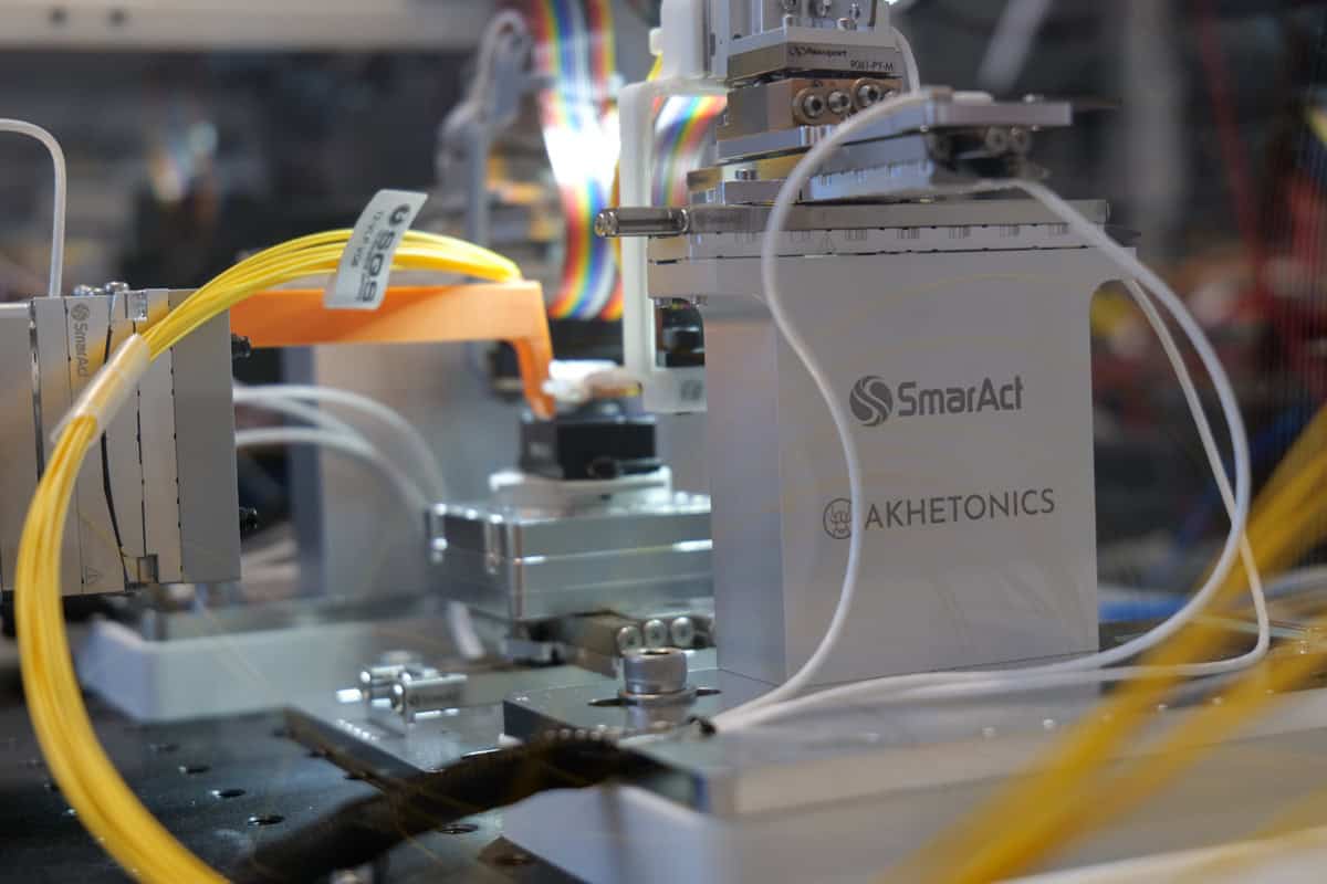
Photonics reimagined SmarAct and Akhetonics worked together to build a versatile optical test set-up to characterize next-generation photonic integrated circuits (PICs). SmarAct’s nanopositioning systems form the precision-motion core of the test workstation, while the positional reproducibility allows Akhetonics to map the full optical chip and evaluate large grids of test components rapidly and reliably. (Courtesy: Akhetonics)
German technology start-up Akhetonics is reimagining the future of high-performance computing (HPC), deploying its proprietary know-how in photonic-design automation and photonic integrated circuits (PICs) to realize the first all-optical digital computation devices. The end-game: an all-optical digital processor – what Akhetonics calls its reasoning processing unit (RPU) – that will fundamentally transform the way that data is processed, transmitted and stored at every level of the HPC stack.
While the anticipated upsides of photonic computing are compelling – think bandwidth scaling, energy-efficiency and reduced latency – the translation of Akhetonics’ R&D effort and early-stage PIC designs into at-scale implementation is still in its infancy. What’s evident even now, though, is that the start-up’s progress is being accelerated by collaboration, interdisciplinary expertise and innovation spanning photonic system design and precision-motion and control technologies.
Collaboration, co-development, customization
A case study in this regard is Akhetonics’ partnership with SmarAct, a German manufacturer and developer of specialist products for nano- and picometre-precise positioning, metrology and automated assembly. Both companies are shaping the future of photonics, albeit along complementary tracks: Akhetonics with its vision of a full-stack photonic computing architecture; SmarAct with a portfolio of enabling technologies that’s helping to make next-generation optical computing a practical proposition.
The two vendors began working together after an initial meeting four years ago at the European Conference on Optical Communication (ECOC 22) in Basel, Switzerland. Top of the Akhetonics shopping list: a versatile optical test system to characterize its advanced PICs.
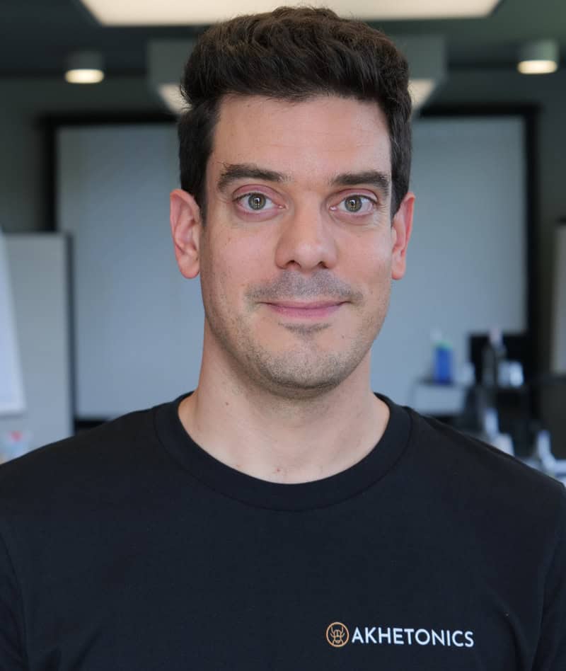
Versatility is the key Leonardo Del Bino, Akhetonics’ CTO. (Courtesy: Akhetonics)
“There are off-the-shelf PIC characterization systems on the market, but they all impose constraints on our design options,” explains Leonardo Del Bino, co-founder and chief technology officer (CTO) at Akhetonics. “Instead, we teamed up with SmarAct to co-develop a compact and modular test architecture built to our exacting specifications. The resulting set-up gives us the flexibility to evaluate and optimize all sorts of innovative PIC designs.”
At the heart of the Akhetonics optical testing workstation sit two discrete nanopositioning subsystems: an XY-Rz chip platform (itself comprising three nanopositioning stages offering horizontal translation along the X and Y axes and rotation limited to the Z axis) and a Z-Rx-Ry “pivot” for an optical probe (where translation occurs only along the Z axis, with simultaneous angular rotation around the X and Y axes). The test set-up (which also incorporates a digital microscope for PIC inspection and alignment) can be used without restriction in every degree of freedom, with the two subsystems working in tandem to ensure precise multi-axis positioning for optical coupling and electro-optic characterization tasks.
On a more granular level, each nanopositioning subsystem is based on SmarAct positioners equipped with integrated optical encoders (SmarAct’s METIRIO® sensors with a resolution of 1 nm) along all six axes of motion. The first subsystem provides three degrees of freedom for lateral alignment (with 49 mm travel in both X and Y, 360° rotation around Rz and a unidirectional positional repeatability of ±40 nm per linear axis). The second subsystem provides vertical and angular alignment (with 31 mm travel in Z, ±5° tilt around Ry, ±45° rotation around Rz and a unidirectional positional repeatability of ±40 nm for the linear Z axis).
To evaluate new PIC designs, Akhetonics’ optical test routines focus primarily on measuring and minimizing insertion losses between input/output fibres and on-chip planar waveguides. Typical measurements include wavelength- and polarization-dependent coupling losses (for example, when a fibre array couples laser light into a series of on-chip grating couplers or when light is coupled from a planar waveguide back into an optical fibre). The subsequent integration of electrical probes into the test system (using two separate XYZ probe towers) supports electro-optic characterization of key on-chip building blocks like optical modulators and photodetectors.
“The requirements for the electro-optical testing are nothing crazy,” says Del Bino. On-chip electrical contacts are in the ballpark of 100 μm x 100 μm, so Akhetonics engineers need positional and alignment precision an order-of-magnitude better than that for their electrical probes. “On-chip optical testing is a different story,” he adds. “A fibre-waveguide mismatch of 1 μm means significant coupling losses, so we need positional accuracy and repeatability of tens of nm or less.”
The rewards of reciprocity
Operationally, the custom test system is the result of ongoing collaboration between the engineering team at Akhetonics and the product development team at SmarAct. After firming up performance requirements, the two vendors iterated back-and-forth with 3D CAD drawings before converging on a final agreed system design.
Line-of-sight Max Trippel, SmarAct’s business development manager for photonic applications. (Courtesy: SmarAct)
“We supplied the nanopositioning stages that form the precision-motion core of the workstation,” explains Max Trippel, SmarAct’s business development manager for photonic applications. Akhetonics then integrated these modules into its own test environment, including the fibre and fibre-array-unit holders; the required optical and electrical measurement equipment; and the software routines for photonic characterization. “This approach gives Akhetonics the flexibility to build exactly the test workflow it needs, while relying on a stable and repeatable positioning platform,” Trippel adds.
Crucially, the SmarAct software “ecosystem” and Python interface make it easy to integrate the nanopositioning stages within Akhetonics’ PIC test routines. That software application platform, known as the SmarAct Control and Process Environment (SCoPE), also creates opportunities for continuous process improvement and product innovation (for example, the ability to develop custom routines for fast calibration and alignment on all axes).
In this way, SCoPE will be a natural fit as Akhetonics transitions its PIC testing programme from an R&D setting through small-batch production runs and, ultimately, to volume manufacturing capability (see “SCoPE in brief”, below). “Our goal with SCoPE is to provide customers with easy access for system development, whether that’s for the testing or assembly of photonic components,” says Trippel. “SCoPE is a living platform and we’re constantly integrating novel functionalities and application-specific plug-ins as well as features to facilitate control of third-party devices.”
Strategically, the SmarAct-Akhetonics partnership is shaping up as a win-win for the long term, with the latter’s growth trajectory and evolving platform technologies feeding into SmarAct’s product development roadmap. “Our customers’ success is our success,” Trippel concludes. “Working in this way with Akhetonics and its peers means we have line-of-sight on ‘what’s next’ in photonic computing. Watch this space: the last word has not been spoken.”
SCoPE in brief
The SmarAct Control and Process Environment (SCoPE) is a modular and extensible software application platform that combines visual process modelling, Python scripting and hardware integration. SCoPE enables customers to develop, control and run automated processes in a unified environment that offers…
Reciprocal benefits The custom test system is the result of an ongoing collaboration between the engineering team at Akhetonics and the product development team at SmarAct. (Courtesy: SmarAct)
Process modelling and automation: visual drag-and-drop process editor enables intuitive creation, control and execution of automation workflows. Live process display gives users direct feedback during execution.
Python scripting backend: integrated Python scripting allows developers to extend workflows with custom logic, algorithms and third-party devices to create advanced automation scenarios. Package and dependency management are built-in.
Device control and hardware integration: native support for SmarAct hardware such as positioning systems, controllers, grippers and interferometers through specialized plug-ins.
Custom user interfaces: flexible Qt widget integration makes it possible to build tailored graphical user interfaces for specific applications.
Data visualization and imaging: configurable plotting widgets, real-time data visualization, process messaging and an integrated image processing pipeline support instant process feedback and image-based automation tasks.
Plug-in architecture: the modular plug-in system enables SmarAct and third parties to extend SCoPE with additional functions, algorithms, hardware integrations or communication interfaces.




 This podcast is supported by