Ultrathin and flexible solar cells could be one step closer thanks to an international team of researchers that has made photovoltaics from 2D crystals called semiconducting transition-metal dichalcogenides (TMDCs). These devices could someday coat any surface exposed to sunlight to produce electricity – something that has proved difficult to do with current solar-cell technologies, which are thick, heavy and brittle.
TMDCs are layered materials with each layer comprising three atomic planes. The outer two planes are triangular lattices of atoms from the chalcogen group of elements – sulphur, selenium, tellurium – that sandwich an inner triangular lattice of transition-metal atoms. TDMCs show great promise for solar-cell applications because electrons within the material interact exceptionally strongly with light. This means that even though these materials are just a few atoms thick, a large portion of the absorbed photons can be used to produce electric current.
“If this technology is developed further, it has a chance of becoming a game-changer in the area of solar energy,” says team member Antonio Helio Castro Neto of the National University of Singapore. The group also included Andre Geim and Kostya S Novoselov from the University of Manchester in the UK and researchers in Portugal, South Korea and Germany.
“Hi-tech sandwich”
Castro Neto and colleagues made a heterostructure, or “hi-tech sandwich” as they call it, containing atomically thin materials, each with a well-defined role. The first component, boron nitride, is a one-atom-thick transparent insulator and it encapsulates the entire ensemble. As such, it is described as the “bread” in the sandwich. Next is graphene, a 2D sheet of conducting carbon that plays the role of the “lettuce”. It is used to collect the electrons produced by the TMDCs (which are the “meat” in the sandwich).
“We also employed gold nanoparticles, which you can think of as the ‘pepper’,” explains Castro Neto. “Although not strictly needed, these particles do ‘spice’ things up by increasing the amount of light absorbed by the structure thanks to a phenomenon called plasmonics.”
The various materials in the sandwich structure all have different electronic properties. “Separately, they are not particularly good for photovoltaic applications but put them all together in a certain combination and you get a very ‘juicy’ photovoltaic device,” says Castro Neto.
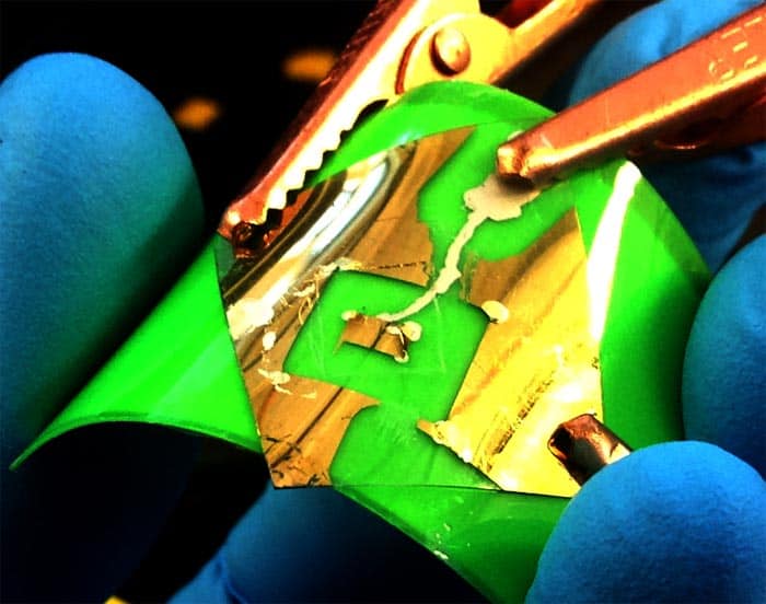
As a case in point, the researchers succeeded in fabricating extremely efficient flexible devices with a photoresponsivity above 0.1 A/W, which is equivalent to an external quantum efficiency of above 30%. The latter means that more than 30% of the light that falls on the cell is converted to an electric current – and it is an important parameter that determines the overall efficiency of how a device converts solar energy to electrical energy.
Extremely sensitive electrons
According to the team, it is so-called Van Hove singularities in the TMDCs that allow for enhanced light–matter interactions. These are named after the Belgian physicist Léon van Hove, who in 1953 discovered that electrons travelling freely through certain crystals could come to a standstill at specific wave frequencies and wavelengths. The electrons essentially “freeze” and their speed reduces to zero. “In this standstill state, the electrons become extremely sensitive to any kind of external stimulus,” says Castro Neto. This results in improved photon absorption and more electron–hole pairs (or excitons) being created in the device. These excitons are responsible for producing electricity – when the electrons and holes separate.
“When light with the right frequency then hits electrons in this unique Van Hove state, they respond massively. This is what we observed in our experiments and we exploited the singularity to boost light absorption and create electric current,” says Castro Neto.
The researchers say that they are now busy looking for materials with stronger Van Hove singularities so that they can increase light absorption even further and improve overall quantum efficiencies. “We are also keen to produce such materials artificially,” reveals Castro Neto. “At the moment, we extract the atomically thin layers from 3D crystals, but we know that there are ways to grow 2D layers artificially and this will be fundamental for technological applications.”
“This is a field that is very much in its infancy,” he adds. “If the graphene field is young – less than 10 years – then this new one is even younger. There is much to do and explore,” he says.
The research is described in Science.