The unique mechanical and electronic properties of multiwall nanotubes are proving to be a rich source of new physics and could also lead to new applications in materials and devices, say Christian Schönenberger and Laszlo Forró
In 1991 Sumio Iijima used a high-resolution transmission electron microscope to study the soot created in an electrical discharge between two carbon electrodes at the NEC Fundamental Research Laboratory in Tsukuba, Japan. He found that the soot contained structures that consisted of several concentric tubes of carbon, nested inside each other like Russian dolls.
A year later Thomas Ebbesen and Pulickel Ajayan, also working for NEC in Tsukuba, developed a highly efficient way of making large quantities of these multiwall nanotubes. Subsequently, in 1993, Iijima’s group at NEC and Donald Bethune’s group at IBM’s Almaden Research Center in California independently discovered single-wall nanotubes. Whereas the multiwall nanotubes were tens of nanometres across, the typical diameter of a single-wall nanotube was just one or two nanometres. The past decade has seen an explosion of research into both types of nanotube.
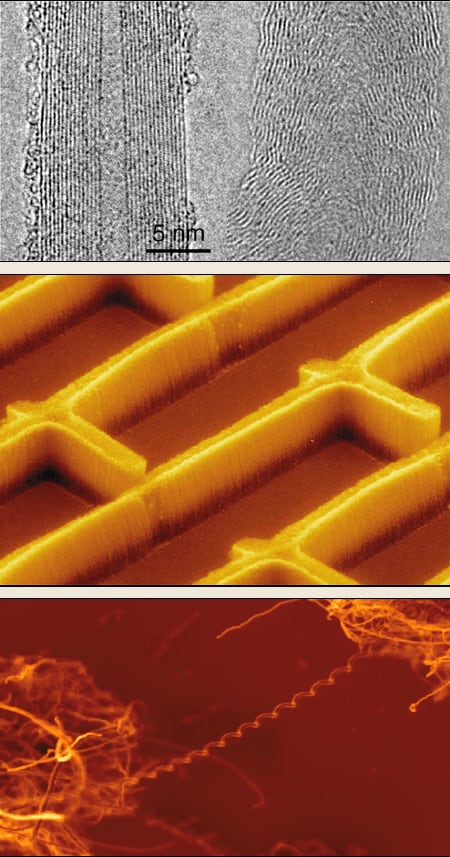
Today, nanotubes can be grown efficiently by the catalytic decomposition of a reaction gas that contains carbon, with iron often being used as the catalyst. This process has two main advantages. First, the nanotubes are obtained at much lower temperature, although this is at the cost of lower quality. Second, the catalyst can be grown on a substrate, which allows novel structures, such as “nanobrushes”, to be obtained (figure 1). Currently nanotubes can be grown to lengths exceeding 100 microns, and in various shapes such as “nanosprings”.
A nanotube can be considered as a single sheet of graphite that has been rolled up into a tube. The electronic properties of the resulting nanotube depend on the direction in which the sheet was rolled up. Some nanotubes are metals with high electrical conductivity, while others are semiconductors with relatively large band gaps. Nanotubes also have remarkable mechanical properties that can be exploited to strengthen materials or to act as “tips” in scanning probe microscopes. And since they are composed entirely of carbon, nanotubes also have a low specific weight.
Mechanical properties
In a sheet of graphite each carbon atom is strongly bonded to three other atoms, which makes graphite very strong in certain directions. However, adjacent sheets are only weakly bound by van der Waals forces, so layers of graphite can be easily peeled apart – as happens when writing with a pencil. As we shall see, it is not so easy to peel a carbon layer from a multiwall nanotube. Carbon fibre is already used to strengthen a wide range of materials, and the special properties of carbon nanotubes mean that they could be the ultimate high-strength fibre.
In 1996 Michael Treacy and Ebbesen, now at NEC Research in Princeton, and Murray Gibson from the University of Illinois in Urbana, measured the Young’s modulus of multiwall nanotubes. The Young’s modulus of a material is a measure of its elastic strength. Treacy and co-workers arranged multiwall nanotubes vertically on a surface so that the tubes were fixed at the bottom and free to move at the top, and then used a transmission electron microscope (TEM) to measure the thermal vibrations of the free ends. The measured vibration amplitude revealed an exceptionally high elastic Young’s modulus of about 1012 newtons per square metre (or one terapascal) – about five times the value for steel.
It is now known that the Young’s modulus should approach a value of 1.25 terapascals. This is true both for multiwall and single-wall nanotubes because the modulus is mainly determined by the carbon-carbon bonds within the individual layers. This value has recently been confirmed by Charles Lieber and co-workers from Harvard University, who used a scanning force microscope (SFM) to bend nanotubes that were mechanically fixed at one end. The scanning force microscope can image, manipulate and measure the force needed to bend the tubes.
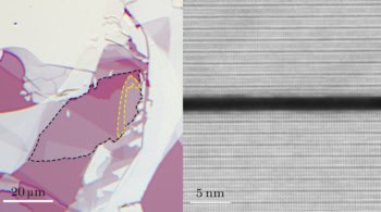
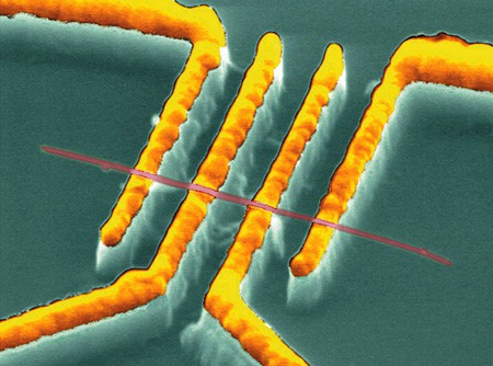
The bending stiffness can also be measured by placing the nanotubes across “nanopores” and using an atomic force microscope to bend them in the middle – a technique developed by Jean-Paul Salvetat and co-workers from the École Polytechnique Fédérale de Lausanne (EPFL) in Switzerland. Salvetat and co-workers began by depositing nanotubes from a liquid onto a well-polished alumina membrane that contained pores about 200 nm across (figure 2). Occasionally a nanotube spanned one of the pores and the microscope was used to measure how the deflection, which is inversely proportional to the Young’s modulus, varied with the applied force.
Salvetat and co-workers found that multiwall nanotubes grown by arc discharge had a modulus of about 1 terapascal, whereas those grown by the catalytic decomposition of hydrocarbons had a modulus that was smaller by one to two orders of magnitude. These results demonstrate that only highly ordered and well-graphitized nanotubes have a stiffness comparable to graphite, whereas those grown by catalytic decomposition have many more defects. (By well graphitized we mean that the carbon-carbon bonds within each layer are strong, while the interactions between layers are weak.) TEM images indeed reveal that the carbon sheets are neither continuous nor parallel to the tube axis.
Lieber and co-workers went on to explore larger forces and deformations, and compared carbon nanotubes with nanorods made from silicon carbide, another very strong material. What they found was surprising: whereas the silicon-carbide nanorods eventually fractured, the multiwall carbon nanotubes buckled, but did not break. This behaviour has since been confirmed in several experiments in which the nanotubes are either bent or compressed along their length.

Euler was the first to calculate what happens to a rod when it is compressed along its length (so-called axial compression). Initially the rod remains straight as the compression increases, before flipping into a curved form at the Euler limit. If this experiment is performed with a drinking straw at constant load, the straw will suddenly develop kinks, which remain if the load is removed. In other words, the kinks are plastic rather than elastic deformations.
Carbon nanotubes are different: first they will bend over to surprisingly large angles, before they start to ripple and buckle, and then finally develop kinks as well. The amazing thing about carbon nanotubes is that these deformations are elastic – they all disappear completely when the load is removed.
To see how these properties might be useful, imagine owning a BMW car made from carbon nanotubes and being unlucky enough to crash into a wall. Due to the high force of the impact, the nanotubes would bend and then buckle, squeezing your BMW into the shape of something like a Volkswagen Beetle. This would happen over a relatively long distance, which would provide an effective “crunch zone”. Moreover, after the crash all the buckles and kinks would unfold and your BMW would “reappear” as if nothing had happened! To be completely safe, however, the nanotubes would have to be combined with energy-absorbing materials, otherwise the collision between the car and the wall would be completely elastic and you would rebound from the wall with the same speed as you hit it!
Other, less futuristic applications might include lightweight bullet-proof vests and earthquake-resistant buildings, while nanotube tips for scanning probe microscopes are already commercially available.
Further insights into the mechanical properties of multiwall nanotubes emerged recently when Rodney Ruoff of Washington University in St Louis and co-workers attached the ends of a multiwall nanotube to a pair of AFM tips and stretched it until it broke (figure 2). They found that the tensile strength was at least an order of magnitude lower than would be expected if the stress was uniformly distributed over all the layers of the nanotube. The outermost layer had to take most of the stress because the tips only made contact with the outside of the nanotube. Ruoff and co-workers found that the outermost tube ruptures at the tensile limit, and that this is followed by a sudden elongation. From TEM images, they concluded that the ruptured outer tube then slides over the inner tubes.
The high strength of carbon nanotubes makes them promising candidates in reinforcement applications, but there are many outstanding problems that must be overcome. First, the properties of the individual tubes must be optimized. Second, the tubes must be efficiently bonded to the material they are reinforcing (the matrix) so that they actually carry the loads. Third, the load must be distributed within the nanotube itself to ensure that the outermost layer does not shear off.
Electronic properties
Carbon nanotubes are giant molecular wires in which electrons can propagate freely, just as they do in an ordinary metal. This contrasts strongly with conventional “conducting” polymers in which the electrons are localized. These molecules are actually insulators and only become conductors if they are heavily doped. Graphite, on the other hand, can conduct electricity because one of the four valence electrons associated with each carbon atom is delocalized and can therefore be shared by all the carbon atoms.
However, it turns out that a single sheet of graphite (also known as graphene) is an electronic hybrid: although not an insulator, it is not a semiconductor or a metal either. Graphene is a “semimetal” or a “zero-gap” semiconductor.
This peculiarity means that the electronic states of graphene are very sensitive to additional boundary conditions, such as those imposed by rolling the graphene into a tube. It can be shown that a stationary electron wave can only develop if the circumference of the nanotube is a multiple of the electron wavelength. This boundary condition means that a nanotube is either a true metal or a semiconductor – a fact that has been confirmed in experiments with single-wall nanotubes.
One would expect to find more complex behaviour for multiwall nanotubes because of interactions between adjacent layers, and this is the subject of ongoing research. Moreover, by combining different nanotubes, and supplementing them with gate electrodes, there is the potential to make a wide variety of electronic devices, ranging from quantum wires to field effect transistors.
On the fundamental side, a perfect metallic nanotube should be a ballistic conductor: in other words, every electron injected into the nanotube at one end should come out the other end. Although a ballistic conductor does have some resistance, this resistance is independent of its length, which means that Ohm’s law does not apply. Indeed, only a superconductor (which has no electrical resistance whatsoever) is a better conductor.
A defect-free carbon nanotube is like an optical fibre. Fibres with large cores are called multi-mode fibres because several wavelengths (or eigenmodes) are allowed to propagate, usually at different speeds, along the fibre. For data transmission, so-called single-mode fibres are preferred because they allow for higher data rates. A single-wall nanotube is almost a single-mode fibre for electrons. Theory predicts the existence of two propagating eigenmodes for a single-wall nanotube, independent of its diameter. The electric conductance (the inverse of the resistance) is then expected to be twice the fundamental quantum of conductance, G0 = 2e2/h, where e is the charge on the electron and h is the Planck constant. This means that nanotubes are predicted to have a minimum resistance of about 6500 Ohms, independent of their length.
One-dimensional conductors are also predicted to have unusual electronic properties that cannot be explained by Fermi-liquid theory – the theory that can predict the properties of most materials. Here, we will concentrate on two recent experiments that address the question of whether multiwall nanotubes are ballistic or diffusive conductors.
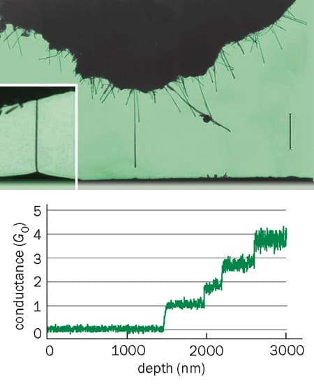
In 1998 Walt de Heer and colleagues at the Georgia Institute of Technology in the US invented an ingenious way to measure the electrical conductance of multiwall nanotubes. A macroscopic fibre of multiwall nanotubes was gently lowered into a drop of liquid metal (figure 3). Because individual nanotubes stick out from the fibre, it is possible, by dipping the nanotubes to different depths, to determine the resistance of individual nanotubes. This technique also allows any variation of resistance with length to be detected.
This method for making electrical contact with nanotubes is very different to techniques that rely on sub-micron fabrication technology (see, for example, figure 4). Quantized conductance will only be observed if ideal contacts are made to the nanotube, and these can be very difficult to achieve. (In an ideal contact none of the electrons entering or leaving the nanotube will be backscattered by the contact.) Early experiments with microfabricated contacts found strong evidence that electrons were scattered. The transport therefore appeared to be diffusive rather than ballistic.
However, de Heer and co-workers found that all multiwall nanotubes have nearly the same conductance, G0 = 2e2/h, and that the dependence of the resistance on length was very weak. In other words, multiwall nanotubes appeared to be ballistic conductors, despite the interactions expected between the different layers (figure 3).
Moreover, the electrical current that could be passed through a multiwall nanotube corresponded to a current density in excess of 107 amps per square centimetre. If nanotubes were classical resistors, the power dissipated by such a current would heat the nanotube so much that it would vaporize. The fact that this does not happen suggests that the electrons in nanotubes are strongly decoupled from the lattice. “Hot” electrons are efficiently removed by the liquid-metal contact rather than being converted into lattice vibrations.
Since multiwall nanotubes consist of several concentrically arranged single-wall nanotubes, one would not expect them to behave as one-dimensional conductors. If adjacent carbon layers interact as in graphite, electrons would not be confined to one layer. The results from de Heer and co-workers suggest, however, that the current mainly flows through the outermost layer, and experiments by the authors in Basel and at EPFL confirm this. It appears therefore that the inner layers only provide mechanical support, although this might change if we were able to make electrical contact with all the layers. However, the question of whether the electron transport is ballistic or diffusive remains unresolved.
Nanotubes and magnetic fields
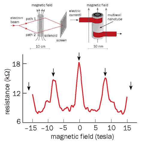
Nanotubes have also been used to help demonstrate the Aharonov-Bohm effect, one of the most fundamental phenomena in quantum physics. In the Aharonov-Bohm effect a beam of quantum particles, such as electrons, is split into two partial beams that pass on either side of a region containing a magnetic field, and these partial beams are then recombined to form an interference pattern. The interference pattern can be altered by changing the magnetic field – even though the electrons do not come into contact with the magnetic field (figure 5).
The observation of the interference pattern demonstrates that a single electron does not choose a particular path but behaves as an extended wave and follows both paths simultaneously. The interference pattern shifts as the magnetic field changes, returning to the original pattern when the magnetic flux has changed by the quantum of magnetic flux, f0 = h/e.
The Aharonov-Bohm effect is particularly interesting because it depends on the electromagnetic vector potential, A, which is related to the magnetic field, B, through the equation, B = curl A. Originally it was thought that the vector potential, A, did not have a physical meaning (various quantities can be added to A without the value of the physical observable, B, being changed). However, the theoretical prediction of the Aharonov-Bohm effect, and its subsequent confirmation in experiments, showed that this is not the case.
Imagine a carbon nanotube placed in a magnetic field with its axis parallel to the field (figure 5). Since nanotubes are cylindrical conductors, the electrons can propagate in either the clockwise or the anticlockwise direction. These two “paths” interfere, resulting in a periodic modulation of the electrical resistance as the magnetic flux through the tube is changed. In this case the period is f0/2 = h/2e. This effect is relatively robust and can be observed even if the electron transport in the nanotube is diffusive.
Last year a collaboration between the authors’ groups at Basel and the EPFL measured the electrical resistance of multiwall nanotubes as a function of temperature and magnetic flux. There was a resistance peak at B = 0, and smaller peaks at B = ±8.5 T, in good agreement with the predictions of the Aharonov-Bohm effect.
Moreover, the value of the magnetic field at the peaks showed that the current was carried by the outermost layer of the nanotube. We note that the magnetic flux through the tube is simply the product of the magnetic field and the cross-sectional area of the tube. The separation of the peaks, DB, and the nanotube radius, r, are therefore related by a simple equation: DB = h/(2epr2). For DB = 8.5 T we find that r = 9 nm, which agrees with direct measurements of the radius with an atomic force microscope. Since a single-wall nanotube has a radius of just a few nanometres, a much larger magnetic field – much larger than is experimentally possible today – would be needed to observe the effect in this system.
The amplitude of the observed Aharonov-Bohm oscillations suggests that the transport is not ballistic in these experiments: in an ideal ballistic nanotube the difference in the resistance at the peaks and the troughs would be much larger. This is because the relative phase of the wavefunction around the circumference determines whether the nanotube is a metal or a semiconductor. Since the magnetic flux changes the phase, a metallic nanotube should continuously evolve into a semiconducting one and vice versa with a flux period of h/e (i.e. twice the period of the Aharonov-Bohm effect). At low enough temperatures the resistance should approach infinity, as the semiconductor would effectively become an insulator. However, this metal-to-semiconductor transition has not been observed in experiments yet.
This and other magneto-resistance measurements show that the electron transport is diffusive, with the scattering length ranging from 3 nm (very diffusive) to 100 nm (intermediate between diffusive and ballistic). The reason for such a wide range of behaviours is puzzling, as is the fact that the metal-to-semiconductor transition has not been observed.
Although transport in multiwall nanotubes is best characterized as diffusive, large electric currents (up to 1 mA) are observed, demonstrating that the electrons couple only weakly, if at all, to the lattice. All these magneto-resistance measurements can be understood in terms of Fermi-liquid theory by assuming the transport is diffusive in two dimensions. However, recent tunnelling experiments in multiwall nanotubes by our Basel-EPFL collaboration have revealed anomalies similar to those seen in single-wall nanotubes. New approaches that go beyond Fermi-liquid theory, such as the Luttinger-liquid model, will be needed to explain these results.
Another breakthrough in the electronic properties of nanotubes was the recent demonstration of “spin transport” by Kazuhito Tsukagoshi of the RIKEN laboratory in Japan, Bruce Alphenaar of Hitachi in Cambridge and Hiroki Ago of Cambridge University. Spin transport will be a key feature in “spintronic” devices that exploit the spin rather than the charge of electrons. Tsukagoshi and colleagues attached layers of cobalt, a magnetic metal, to opposite ends of a multiwall nanotube, and showed that the resistance of the nanotube depended on the relative orientation of the magnetization in the two cobalt layers. For this to happen, the direction of the electron spins must be maintained as they move along the nanotube, a property that could prove to be very useful in spintronics.
Field emission
The small diameter of carbon nanotubes is very favourable for field emission – the process by which a device emits electrons when an electric field or voltage is applied to it. The use of nanotubes as field emitters was first proposed by de Heer, André Chatelain and Daniel Urgate in 1995. Field emission is important in several areas of industry, including lighting and displays, and the relatively low voltages needed for field emission in nanotubes could be an advantage in many applications. However, as with all new technologies, there are formidable obstacles to be overcome.
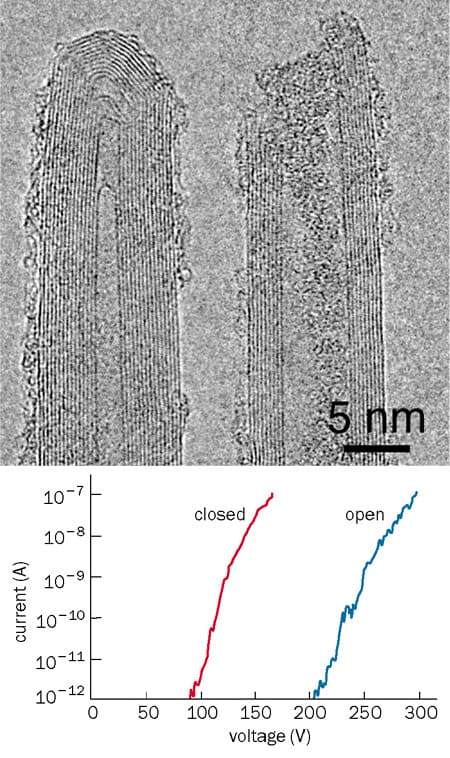
Here, we will focus on measurements of field emission from different types of nanotubes by Jean-Marc Bonard and co-workers at EPFL. To make a field-emission source with just one nanotube, individual multiwall nanotubes were mounted onto a gold tip. The nanotubes were kept in place by van der Waals forces alone (i.e. adhesive was not used). Bonard and co-workers compared the field emissions from multiwall nanotubes with open and closed ends (figure 6). Nanotubes grown in arc discharges are normally closed, but they can be opened by applying a very large electric field, or by treating them with oxygen at high temperature. Field emission occurred when a potential of a few hundred volts was applied to the gold tip. Both open and closed nanotubes were capable of emitting currents as high as 0.1 mA, which represents a tremendous current density for such a small object.
Surprisingly, closed nanotubes were much more efficient than open ones (figure 6b). This was surprising because the smaller effective curvature of the open nanotubes was expected to lead to a larger field amplification. It is now thought that other species (such as oxygen atoms) attach themselves to the free dangling bonds at the end of the nanotube, resulting in localized electron states. Since these states lie well below the Fermi energy in the nanotube, they cannot emit electrons. Localized states are also thought to form at the tips of closed nanotubes. However, these states couple to so-called p-orbitals in the nanotube and this effectively enhances the emission of electrons. This also has the advantage of narrowing the energy distribution of the emitted electrons. Electron microscopy is one application in which this effect would be very useful.
Carbon nanotubes exhibit a wealth of properties and phenomena. While many of these are understood, others remain controversial, and nanotubes are sure to remain an exciting area of condensed-matter physics for years to come. The amazing structural and electronic properties of nanotubes are not in doubt. Like any new technology, however, nanotubes will have to outperform current technology to gain a foothold in commercial markets. All these challenges will keep nanotube researchers busy for a long time to come.
Further reading
General articles
C Dekker 1999 Carbon nanotubes as molecular quantum wires Physics Today May pp22-28
M Dresselhaus et al. 1998 Carbon nanotubes Physics World January pp33-38
Mechanical properties
M R Falvo et al. 1997 Bending and buckling of carbon nanotubes under large strain Nature 389 582-84
P Poncharal et al. 1999 Electrostatic deflections and electromechanical resonances of carbon nanotubes Science 283 1513-16
M M J Treacy, T W Ebbesen and J M Gibson 1996 Exceptionally high Young’s modulus observed for individual carbon nanotube Nature 381 678-80
E W Wong, P E Sheehan and C Lieber 1997 Nanobeam mechanics: elasticity, strength, and toughness of nanorods and nanotubes Science 277 1971-75
M-F Yu et al. 2000 Strength and breaking mechanism of multiwalled carbon nanotubes under tensile load Science 287 637-40
Electronic, magnetic and quantum properties
A Bachtold et al. 1999 Aharonov-Bohm oscillations in carbon nanotubes Nature 397 673-75
S Frank et al. 1998 Carbon nanotube quantum resistors Science 280 1744-46
C Schönenberger et al. 1999 Interaction and interference in multiwall carbon nanotubes Appl. Phys. A69 283-295
K Tsukagoshi, B W Alphenaar and H Ago 1999 Coherent transport of electron spin in a ferromagnetically contacted carbon nanotube Nature 401 572-74