Long seen as a reliable workhorse, the scanning electron microscope also has a more exciting side. Debbie Stokes explains why a ‘quiet revolution’ is occurring in some SEM labs.

Since the first commercial instrument debuted in 1964, the scanning electron microscope (SEM) has become an established tool for characterizing materials in the physical and life sciences. SEMs are commonplace in the semiconductor industry, where they are used to create and characterize extremely small features, and the instruments are a key driver in the emerging business of nanotechnology.
The SEM is often seen as being less exciting than its counterpart, the transmission electron microscope (TEM), which can resolve individual atoms. Instead, SEM has a reputation as a workhorse instrument that is reliable, easy to use and ideal for characterizing bulk materials.
However, there has been a quiet revolution in the world of the SEM, and slowly but surely, its capabilities are expanding. The instrument can now be used to study the surface of just about any bulk material at nanometre resolution and regardless of whether it is clean or dirty, wet or dry, hot or cold, conducting or insulating. Under the most favourable conditions, sub-nanometre resolution has been achieved — especially for thin specimens imaged in transmission mode.
An SEM consists of a source of electrons that are focused by lenses into a tight beam that strikes the surface of a sample. The resultant signals from the sample — including backscattered electrons, secondary electrons and X-rays — are picked up by detectors.
Specimen as active component
Radical improvements in SEM capabilities have been brought about by new technologies such as field emission electron sources, magnetic immersion lenses, more efficient and sensitive detectors and specially adapted specimen chambers and stages. In addition, there is a growing awareness in the SEM community that performance can be boosted by treating the specimen as an integral, active component of the system.

So where does all this extra power get us? Well, it opens up a world of possibilities for tuning the experiment to match the specimen; to tease out the required information or to reveal the unexpected; and to use an SEM to fabricate structures at increasingly small scales.
One strategy to improve the performance of an SEM is to apply a negative-bias voltage to the specimen, which slows down the incident (primary-beam) electrons on arrival at the specimen surface. These lower energy electrons don’t penetrate as deeply into the sample as a higher-energy primary beam would, and therefore are a more sensitive probe of the surface. The advantage of using a higher primary energy is that the beam can be made much more tightly focused, resulting in better spatial resolution.
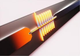
Figure 1 shows this concept schematically, along with an image where the landing energy is a mere 50 eV, compared to the primary-beam energy of 2 keV. The reduced penetration of primary electrons into the material gives a much greater surface-sensitivity and, with the right detector, enables high-quality, low-voltage backscattered electron imaging (figure 2). This technique is unique in that it can provide high-resolution compositional and topographical information at the same time.
Another way of boosting the capability of an SEM is to position a detector beneath a thin specimen in order to collect electrons that are transmitted through the sample — similar to what is done in a scanning TEM (STEM). This “STEM-in-SEM” technique takes advantage of the comparatively low primary beam energies of the SEM (typically less than 30 keV), which means that more of the primary electrons scatter more often as they pass through the specimen.

This increased scattering makes it easier to study materials containing lighter atoms such as carbon, which are not very efficient at scattering electrons. This technique is particularly useful for studying polymers, carbon nanotubes (figure 3) and other organic matter.
Another exciting innovation is the environmental SEM (ESEM), which can also be used in STEM mode. “Environmental” refers to the instrument’s ability to image a sample in its “native state” rather than first being desiccated, coated in gold and held under high vacuum. The ESEM and microscopes using similar technologies are well suited to the study of electrically insulating bulk materials such as oxides, ceramics, glasses and polymer. Such materials would normally be electrically charged by the primary beam, making analysis very difficult.
The technique works by introducing an “imaging gas” such as water vapour to the sample chamber. When the primary beam strikes the sample, it produces ‘secondary electrons’, which ionize the gas, creating more secondary electrons as well as positive ions. The additional electrons serve to amplify the secondary electron signal, while the positive ions are attracted to the sample where they compensate for negative charge deposited by primary electrons.
Wetting and drying cycles
If water vapour is used as the imaging gas, the sample chamber becomes a suitable environment for stabilizing liquid-containing specimens and performing in situ experiments — for example, a sample can be studied as it is put through cycles of wetting and drying. Specimens can also be heated, cooled, stretched, compressed and otherwise manipulated, in association with a range of gases appropriate to the experiment. Recent advances in detector design mean that experiments can be carried out at chamber pressures up to around 4 kPa. While this is not quite atmospheric pressure (101 kPa), the pressure in a normal SEM is typically about one million times lower than this.
The SEM is also playing an increasingly valuable role in the fabrication of nanometre-scale devices for electronics and other applications. For example, interactions of the electron beam with specific gases can be used to achieve the controlled deposition of materials such as metals or different forms of carbon onto a substrate. This technique can be used to build 3D nanostructures or to create connections between nanocomponents.
Another method for making extremely small features using an SEM is electron-beam lithography. This process uses the electron beam to “draw” circuit patterns onto a substrate that is coated with a polymeric photoresist. The surface is then subjected to chemical etching, which removes the polymer that has not been exposed to the electron beam. Deposition and etching techniques can also be combined in a gas-mediated environment, as in the ESEM, leading to new and important techniques for creating nanostructures.
SEM analysis can be enhanced by the integration of a focused ion beam (FIB), which is scanned across the sample much like the electron beam. The FIB can be used to remove material from the surface of the sample (a process called milling), which allows the electron beam to probe deeper into the material. This sequence is repeated a number of times to obtain a number of 2D “slices” through a material, which can later be volume-rendered to create a 3D image. Slices can range in thickness from the nanometres to micrometres, depending on the size distribution of features present in the material. These abilities can be coupled with traditional analytical techniques such as electron backscatter diffraction (EBSD) and X-ray microanalysis (EDS) to build up 3D images of the structural and chemical properties of the sample.
This brief survey has shown how the modern SEM can take us from the advanced characterization of hard and soft materials, even liquids, to 3D visualization, dynamic experiments and the fabrication of nanostructures. Much of this is possible thanks to the extremely high level of control offered by the SEM — an ability that has evolved through decades of technology development coupled with increased computing power and dedicated software. In a cutting-edge world, the not-so-humble SEM is rising magnificently to the challenges of the 21st century.