Daniel Twitchen and Matthew Markham explain why carbon’s most alluring allotrope could be a quantum physicist’s best friend, and how the market for diamond-based quantum technologies is starting to take shape
In the 20th century many aspects of quantum physics were harnessed into world-changing technologies, including semiconductors, lasers and other now- ubiquitous devices. Throughout this first quantum revolution, however, one key aspect of quantum physics – superposition – has largely remained in the laboratory, a fundamental curiosity rather than a promising feature to be exploited.
However, this is about to change, thanks to several significant initiatives that aim to bring about a second quantum revolution. The key to this revolution’s success will be the ability to “easily” engineer and control quantum bits. We use the word “easily” with caution, because initializing a quantum state and keeping it in a superposition for significant lengths of time is a difficult undertaking. Scientists are exploring many different approaches, using materials as varied as superconductors, synthetic diamonds, cold atoms and quantum dots, and the race is currently wide open. But diamond does have some intriguing advantages, both for quantum computation and for other applications such as magnetic-field sensing. The challenge for our organization, the industrial diamond firm Element Six, has been to support research in this area while also staying true to our core business interests in materials applications.
A useful flaw
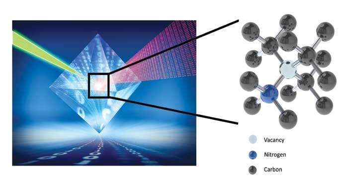
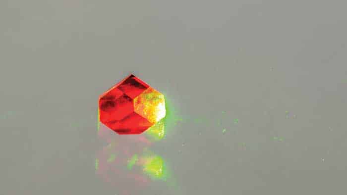
The type of diamond that attracts would-be quantum revolutionaries has a defect in its otherwise uniform lattice of carbon atoms. This defect consists of a single nitrogen atom adjacent to a missing carbon atom, or vacancy. The nitrogen-vacancy (NV) centre has unique optical absorption and emission properties – among other effects, it gives diamond a red-to-pink colouration – and these properties have long been the focus of fundamental research on crystal structures.
In addition to its unusual optical properties, the negative charge state of the NV centre also has an electronic spin, S = 1, in its ground state. Remarkably, the state of this electronic spin can be controlled and read out at room temperature. The reason is that unlike most materials, the crystal lattice in diamond forms a low-noise environment, so fragile quantum properties are not lost and information can be stored and probed for longer time periods. The spin state can be read out by measuring the intensity of light given off by an NV centre as the system is excited by microwave radiation. At the NV centre’s resonance frequency of 2.88 GHz, the spin state will flip from 0 to a +1 or –1, causing a dip in the intensity of red light emitted.
The robustness of this spin state, and the ease of reading it out, make NV diamond a very promising platform for a wide range of quantum technologies, with potential applications in secure communications, computing, imaging and sensing. A recent focus area for the diamond community is the use of NV defects to measure magnetic fields. Thanks to the Zeeman interaction, the gap between the frequencies of the 0 → 1 and –1 → 0 microwave transitions in NV diamond increases as a function of magnetic field. Hence, in the simplest case, one can estimate the magnitude of the magnetic field by exposing the NV centre to a range of microwave frequencies and measuring the separation between the two dips in intensity. Remarkably, a basic measurement of this type can be performed using a single NV centre at room temperature. With multiple NV centres, the geometry of the diamond lattice means that one can make extremely sensitive measurements of the field’s direction as well as its magnitude.
Raw materials
Of course, numerous technologies for estimating magnetic field already exist. These include superconducting quantum interference devices (SQUIDs), vapour cells, flux-gate sensors and the Hall-effect sensors that constitute the compass in modern smartphones. However, SQUID-based magnetometers must be cryogenically cooled, making them relatively bulky and costly to run, while other sensor technologies require frequent recalibration and offer limited frequency bandwidth for measuring changing magnetic fields. In contrast, NV diamond-based sensors do not need to be recalibrated, have a broad bandwidth and could be incorporated into a lightweight, low-powered device. Critically, NV centres can also be used to construct maps of magnetic field across a surface, thanks to the high spatial resolution provided by a microscopic probe. For these reasons, diamond-based magnetometers have strong potential both as replacements for existing technologies and as the enablers of applications where competing technologies do not yet exist.
For these applications to become a reality, though, we need a ready supply of high-quality NV diamonds. NV centres are rare in natural diamonds, and it is difficult to do much research if you are limited to working with a single sample. At Element Six we have developed methods for growing NV diamond synthetically using chemical vapour deposition (CVD). This process involves filling a microwave chamber with a mixture of hydrogen, methane and nitrogen gas, and heating it to 2500–3000 K to create a plasma. Diamond “seeds” placed in the chamber become the nuclei for new diamonds as carbon atoms from the plasma deposit onto their surfaces layer by layer. The hydrogen stabilizes the surface against forming graphite instead of diamond, while the nitrogen acts as a dopant, making it possible for NV centres to form.
This process is the result of more than 15 years of intensive R&D and it enables us to grow diamond in a controlled and scalable fashion, with a purity far exceeding that of natural diamonds. It also makes it possible to control the number of NV centres. Under high-purity conditions, small numbers of NV centres are produced via the chemistry of the growth process. These isolated vacancies can be probed individually in an experiment, so this type of NV diamond is well-suited for quantum- computation applications. Magnetic- sensing applications require higher numbers of NV centres, and we achieve this by increasing the nitrogen concentration during synthesis and then bombarding the crystal with high-energy electrons to create additional vacancies. Heating the diamond to 800 °C causes these vacancies to migrate through the crystal lattice until they encounter nitrogen atoms; at that point, the structure stabilizes, since the NV centre has a lower potential energy than a separate nitrogen and vacancy.
The value chain
Over the past decade advances in our diamond-making capabilities, coupled with a deepening understanding of the physics of quantum spins in NV diamond, have opened up a wide range of potential applications. Element Six has supported this nascent field by supplying state-of-the-art diamond samples and diamond engineering expertise to external partners, while focusing internally on making further improvements to the material. In recent years, however, we have also become more active in supporting commercial start-ups to allow them to incubate the technology and in helping larger companies assess the applicability of our diamonds to various market opportunities.
The breadth and depth of knowledge needed to appreciate these opportunities is significant. It requires one to consider an entire value chain: a material; a device made from that material; the package surrounding that device; the subsystems and systems the device fits into; and finally the user. As is often the case, the commercial value of this chain is concentrated at the subsystem and system level. But Element Six is a materials company, and we have grown by developing novel materials that address problems across multiple markets and industries. Making devices, let alone complete systems for end users, is not really our speciality. So how can we access the value at the other end of the chain?
Rather than changing our strategic focus, we have instead sought to exploit diamond quantum devices by communicating their “value proposition” to end users. A basic demonstration of the NV centre’s ability to measure magnetic field is not difficult, and a prototype device can be made using remarkably simple components such as off-the shelf diode lasers and photodiodes, and coils of wire to deliver the microwaves to the sample. Packaging all of this together into a robust unit is less trivial, of course; ultimately, the performance of a diamond sensor will depend not only on the material itself and Element Six’s expertise, but also on the stability of surrounding components and the data-processing algorithms used to transform raw measurements of light intensity into an accurate and highly sensitive map of the vector magnetic field. Nevertheless, it is always much easier to convince people of a device’s potential with a demo than with PowerPoint slides.
Another component of our strategy has been to partner with university researchers who are developing diamond-quantum-device technology. This has enabled us to secure some intellectual property (IP) on the physics needed to make working devices – although, crucially, we actively avoided filing patents for the actual applications because we wanted to leave third parties free to develop their own. Our university partners have also been an important bridge between us and potential end users. Making a diamond-based quantum device (or indeed any quantum device) requires knowledge of quantum physics, and since this is an emerging industry most organizations do not yet have that expertise. Combining our IP and materials know-how with their quantum-physics expertise enabled us to start talking to organizations that were actually in a position to develop this technology. In addition, many of the academic groups we work with have produced spin-out companies. We have supported these companies with materials sales and knowledge-sharing, and we anticipate that the applications they develop will be a growth area for Element Six over the coming years.
Potential gems
Diamond quantum technologies are extremely promising, with many applications already at the proof-of-concept stage. These include applications in materials characterization such as nanoscale imaging of the write heads for next-generation magnetic hard drives, and biological imaging. New sensing methods for pressure and temperature, plus the alluring possibility of diamond-based quantum computing, makes this an exciting and productive area.
We foresee that diamond will continue to be used as a tool to aid our understanding of the quantum world. However, the real excitement concerns the possible technologies that this understanding will enable. In late 2016 a group of researchers led by Ron Walsworth at Harvard University, US used NV centres in diamond to study neuron activity in marine worms, measuring the tiny magnetic pulses from single neurons with high spatial resolution. No other existing technology can perform measurements at such high sensitivity and resolution; the maximum spatial resolution of standard MRI scans is about 1 mm3, whereas diamond-based magnetic field sensing could, in theory, give us cellular-level images of chemical processes. We expect that this proof-of-principle experiment will be followed by breakthroughs in our understanding of how the brain works, as well as new diagnostic methods and treatments.