Semiconductor nanowires are increasingly used in electronic devices including field-effect transistors, sensors, detectors and light-emitting diodes. More complicated devices are expected soon, requiring new and improved ways of growing such wires. Lincoln J Lauhon and colleagues at the University of Harvard have now synthesised nanowires that are only 50nm in diameter containing a germanium core surrounded by a silicon shell. They also made “triple decker” wires of silicon, silicon oxide and germanium. These so-called “core-shell” and “multi-shell” structures allow a semiconducting wire to be encased in an insulating shell (Lincoln J Lauhon et al. Nature 2002 420 57)
Semiconductor nanowires are one-dimensional structures, with unique electrical and optical properties, that are used as building blocks in nanoscale devices. Their low dimensionality means that they exhibit quantum confinement effects. For example, narrowing the wire’s diameter increases its band gap, compared to the bulk material.
Researchers have examined various ways of growing semiconductor nanowires, including laser ablation, chemical vapour deposition (CVD) and template-assisted growth. While laser ablation and template-assisted approaches provide bulk quantities of semiconductor nanowires, they do not provide much control over the composition, size or crystallographic direction of the nanowire.
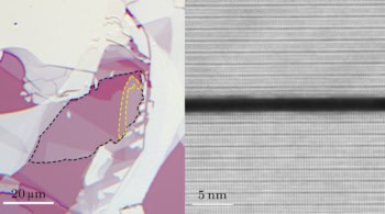
What Lauhon and co-workers have done is to grow core-shell and core-multishell nanowire heterostructures using a CVD method that provides increased control over the structure’s composition. Using their technique, the nanowires are grown by gradually building up thin, uniform shells around a nanometre-sized cluster of gold atoms. The nanowires had boron-doped silicon shells surrounding intrinsic silicon, as well as silicon wrapped around a silicon oxide core. They also investigated the growth of crystalline germanium-silicon and silicon-germanium core-shell heterostructures.
The Harvard group has already used the approach to prepare new devices called nanowire field-effect transistors. Working with researchers from Intel, the team also plans to integrate these transistors with conventional semiconductor processing to produce advanced hybrid devices, “This is quite exciting since it may lead to real-world use of a very basic discovery,” says Charles Lieber, the leader of the group.
The researchers will now look at other materials and believe that the general ideas outlined in their work are applicable to many materials. “One particularly interesting application that we are pursuing is core-shell-shell structures in III-V semiconductor materials such as gallium nitride,” Lieber told PhysicsWeb. “These structures can give rise to very interesting photonic devices.”