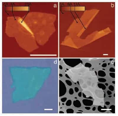
A standard technique for producing two-dimensional crystals just one atomic layer thick has been developed by physicists in the UK and Russia. The crystals, which are essentially gigantic 2D molecules, were created by Andre Geim and co-workers at Manchester University and the Institute for Microelectronics Technology in Chernogolovka. The structures were made by simply rubbing the freshly cleaved surface of a layered crystal onto another surface, like drawing chalk on a blackboard. This micromechanical "peeling" created flakes, some of which were -- unexpectedly -- just one layer thick. The crystals are stable and could be used to make transistors and sensors (Proc. Natl. Acad. Sci. 2005 102 10451).

Geim and colleagues first made 2D crystals last year by peeling layers of graphene — 2D sheets of carbon atoms — from the surface of a thick crystal of graphite. They then used optical, electron-beam and atomic-force microscopy to separate out the thinnest films, which were just one carbon atom thick. The UK-Russia team also used standard lithography techniques to process the films, which have useful electronic properties, to make field-effect transistors (FETs).
Now, however, the group has found that the technique can be used on almost all layered materials, in which individual atomic planes are bound together only weakly. They have, for example, made 2D crystals from boron nitride, several dichalcogenides and various complex oxides. Furthermore, Geim and colleagues found the crystals were stable for several weeks at room temperature and that most of them kept their structural and electronic properties.
“For years there was a discussion if 2D materials should exist or not,” says lead author Kostya Novoselov. “Now that we have proved that 2D crystals exist and that they are stable, we can study their electronic, optical and mechanical properties. And it’s a whole new class of materials, which include metals, insulators, semiconductors and probably magnetic materials.” The discovery will also allow theoretical models of 2D materials to be tested. “These are very exciting materials to work with,” adds Novoselov. “We can study almost any property of matter in 2D.”
Applications include field-effect transistors, highly sensitive gas sensors, electromechanical devices and translational motors.


