Scientists in the US have developed the first method to sort semiconductor carbon nanotubes by size. The technique, devised by Howard Schmidt and colleagues at Rice University, is based on dielectrophoresis and not only separates metallic nanotubes from semiconducting ones but also sorts the semiconducting tubes according to their diameters. The ability to separate and sort nanotubes like this will be essential for making devices from these materials (J. Am. Chem. Soc. in press).

Single-walled carbon nanotubes have enormous potential as the building blocks in high-speed nanoscale electronics. Nanotubes are essentially rolled up sheets of graphite, and they can be metallic or semiconducting depending on the direction in which the sheet has been rolled up. Metallic tubes can function as nanoscale leads, and semiconducting tubes as nanoscale transistors.
However, when single-walled carbon nanotubes are made, a mixture of both metallic and semiconducting nanotubes is produced. Moreover, the semiconducting tubes are produced in a variety of sizes, each of which have different electronic and optical properties. This is because a nanotube’s band gap, which controls its properties, is determined by the tube diameter. Although methods to separate metallic tubes from semiconducting ones have been developed, no such technique for sorting nanotubes by size was available until now.
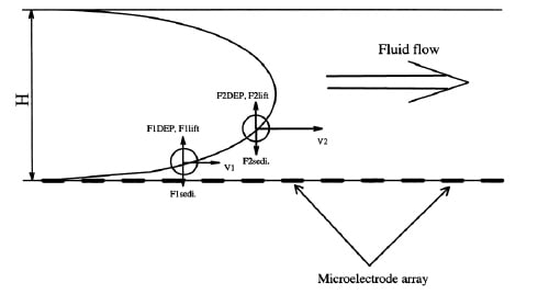
Schimdt and colleagues’ method sorts semiconducting nanotubes according to their dielectric constant (a material’s ability to store electrostatic energy), which in turn depends on their diameter. The Rice team began by making a narrow electrified chamber by wiring an array of microelectrodes, which provide a strongly inhomogeneous electric field, to an AC power source and then pumped a solution containing the nanotube mixture into the chamber using a syringe. They researchers observed that the metallic tubes were attracted towards the microelectrode array while the semiconducting tubes remained in the solution. The two types of nanotubes move in different directions along the electric field gradient (which varies from top to bottom in the chamber) because the semiconducting nanotubes have a smaller dielectric constant than that of the solvent, while the metallic nanotubes have a larger constant.
In addition to this, the semiconducting nanotubes were found to float at different levels in the chamber depending on their diameter: smaller diameter tubes have smaller dielectric constants than larger ones and so floated higher in the chamber while the larger tubes moved lower. The researchers were able to spread out the different-sized nanotubes by simply using the flow gradient close to the electrode array surface. They could do this thanks to the general behaviour of fluids in narrow channels: nanotubes that are drawn close to the electrode array move very slowly in the flow while tubes that are pulled in less ride higher, and thus flow faster (figure 1).
“We expect this process will contribute to the application of single-walled nanotubes in next-generation electronic manufacturing, allowing for selected types of nanotubes to be assembled onto circuits directly from solution,” Schmidt told PhysicsWeb.
The Rice team now plans to perfect and scale up its technique. The scientists eventually hope to build an automated system that can run unattended.


