Porous materials can have unusual properties such as large surface areas, making them ideal as catalysts and sensors. Silicon containing tiny, nanoscale pores can even emit light, even though ordinary silicon cannot. Now two independent groups of researchers in the US have developed techniques to make porous germanium – another semiconductor widely used in microelectronics. The material could be used to make more efficient solar cells and chemical sensors.

Scientists first discovered in the early 1990s that silicon could be made to emit light by etching holes into it. But attempts to make porous germanium — another semiconductor in the same group of the periodic table as silicon — have been less successful, yielding structures with only randomly distributed pores. Now, Sarah Tolbert and colleagues at the University of California at Los Angeles and Gerasimos Armatas and Mercouri Kanatzidis of Michigan State University have used a technique called “surfactant templating” to make germanium containing well-ordered pores for the first time (Nature 441 1126 & 1122).
Tolbert’s team made their porous germanium by taking a compound called K2Ge9, which contains small clusters of nine germanium atoms that link up to form short polymer chains. They then reacted this material with a carbon-containing “surfactant” molecule that, like soap, has a water-loving end and a water-repelling end.
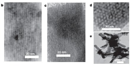
The different electrostatic interactions between the chains of germanium atoms and the two ends of the surfactant molecule cause the germanium atoms to form a hexagonal-shaped honyecomb structure, with the surfactant molecules lying in between as a “scaffold”. The surfactant was then removed by oxidising the sample to leave just the porous, honeycomb germanium (figure 1).
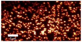
The Michigan team used a similar approach, but with a different germanium compound a different surfactant, to obtain porous germanium with cubic channel structures (figure 2).
Both groups found that the nanoporous germanium absorbs light at shorter “bluer” wavelengths than ordinary crystalline germanium. Moreover, Tolbert’s team found they could “tune” this wavelength by altering the thickness of the walls between pores, converting only some of the germanium to germanium oxide. The researchers also found that this worked for alloys of silicon and germanium – compounds that are routinely used in micro- and optoelectronics.


