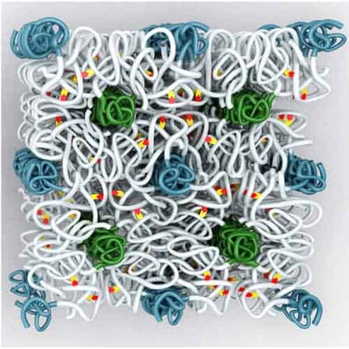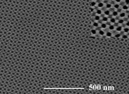
Researchers in the US are the first to use self-assembly to make highly-ordered square arrays from block copolymers. Each square measures about 20 nm and the team believes that the technique could someday be used to make extremely small electronic devices. Until now, block-copolymer self-assembly methods could only produce hexagonal-shaped arrays, which are not compatible with the industrial processes used to make integrated circuits.
Self-assembled square arrays are a major goal for researchers because the semiconductor industry’s circuit design, software and fabrication processes are all based on a rectilinear coordinate system. Although hexagonal patterns can now routinely be produced using conventional self-assembly techniques, adopting these shapes would mean rethinking semiconductor industry protocols, which would be very expensive and time-consuming. To this end, the Semiconductor Industry Association has set up a challenge to scientists working in the field of “block copolymer” lithography to develop square arrays of etchable block copolymer domain patterns.
Integrating the new technique into semiconductor manufacturing will be much simpler and will not require any modification to chip designs or layouts Craig Hawker, UCSB
Block copolymer lithography is a simple approach to make features smaller than 20 nm, which is less than half the size of today’s smallest mass-produced circuits. Block copolymers are two different kinds of polymer strand (called blocks) that are joined end-to-end to create one long strand. Although the ends of the blocks are stuck together, the blocks tend to repel each other along their length. These competing forces tend to organize the copolymers into well defined patterns with length scales of tens of nanometers.
A thin film of block copolymers on a semiconductor substrate provides the initial nanostructure pattern. Then a chemical treatment can be used to remove one type of block, exposing some of the substrate and creating a mask that can be used create devices through standard lithography processes such as etching and deposition. Feature sizes can be controlled by adjusting the molecular weights of the blocks — however, the traditional way of creating the films by the phase separation of the polymers automatically leads to hexagonal arrays of features.
Two copolymers are better than one
The new technique developed by a multidisciplinary team at the University of California, Santa Barbara is very similar to block copolymer lithography but involves using an mixture or “alloy” of two different block copolymers that have an attractive hydrogen-bonding interaction with each other (Sciencexpress 10.1126/science.1162950).
The block copolymers used by the team were based on polyethylene oxide-b-polystyrene (PEO-PS) and polymethylmethacrylate-b-polystyrene (PMMA-PS). Such a blend combines the photodegradability of the PMMA with the long-range ordering characteristics of the PEO. Hydrogen-bonding occurs between phenolic and pyridyl units in the copolymers. Degrading the PMMA domains using UV light, followed by etching, allows nanoscale features to be made with high fidelity, which leads to highly-ordered square arrays that are around 20 nm across.
Simple integration
“The square arrays produced match the layout of microelectronics devices,” team member Craig Hawker told physicsworld.com. “As a result, integrating the new technique into semiconductor manufacturing will be much simpler and will not require any modification to chip designs or layouts.”
The team now plans to make features over larger areas and fabricate devices using a combination of traditional processing techniques and square arrays produced by block copolymer lithography.


