Physicists in the US and Germany have developed a new approach for making tiny structures that could someday be used in electronic devices.
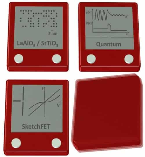
The team has used the technique to fabricate transistors with features at sizes of just 2 nm — which they have dubbed “SketchFETs”. What’s more, the devices can be erased and reformed as desired, a result that could be important for nanoelectronics applications.
Most transistors today are made from silicon using optical lithography, but it is difficult to shrink these devices to below about 20 nm.
The new technique, developed by Jeremy Levy and colleagues at the University of Pittsburgh and University of Augsburg, can produce features that are 10 times smaller in linear terms and 100 times smaller in terms of area than devices at the end of the “roadmap” for commercial silicon devices, says Levy.
The technique, which was first described last year, involves using the probe of an atomic force microscope to sketch conducting paths, or wires, just a few nanometres across, at the interface of a crystal of strontium titanate and lanthanum aluminate (both of which are insulators).
Potential for memory devices
The wires can then be erased using a reverse voltage or with light, which renders the structure insulating again. It is the reversible nature of the process that makes it potentially useful for applications like memory devices, explains Levy.
Now, the team has taken its technique a step further by fabricating tiny field-effect transistors and tunnel junctions as well as just conducting wires on an insulating substrate (Science 323 1026). Because these devices measure just 2 nm across, many of them can be packed into a given area.
According to the researchers, this new route to nanoelectronics will be important for making high-density memories, chemical sensors and computer processors.
And that’s not all: because the devices approach the atomic scale, they can be used to study quantum mechanical phenomena such as tunnelling. Understanding such behaviour will be crucial for modelling novel electronic materials and perhaps even for making quantum computers in the future.


