A technique for producing extremely smooth patterns has doubled the distance that surface plasmons can travel on metal films, according to researchers in the US. The “template stripping” approach also simplifies how the films are made, and relies largely on inexpensive silicon wafers and adhesives, claims the team. The research could lead to a practical way of manufacturing new types of solar cells and other “plasmonic” devices that exploit interactions between light and electrons.
Surface plasmons propagate on the surface of a metal as collective oscillations of electrons — and they can interact strongly with light. When light strikes a flat metal surface at right angles it will not excite plasmons, but creating patterns on the surface allows this excitation, as long as the pattern dimensions are smaller than the wavelength of the light.
Unfortunately, plasmons are also scattered and absorbed by irregular bumps on a surface, reducing the effectiveness of roughly-hewn plasmonic devices. Techniques traditionally used to fabricate nanostructures — which can involve painstakingly carving out patterns with an ion beam — produce surfaces that are too uneven. Ions implanted as a side-effect of this technique also lead to plasmon absorption.
Serendipity strikes
Now David Norris and colleagues at the University of Minnesota have developed a method that deposits copper, gold or silver onto a patterned silicon template wafer. They then apply an adhesive to the imprinted metal, and pull the metal and adhesive together away from the silicon to create an extremely smooth yet patterned surface.
“This template stripping method is very well known in scanning tunneling microscopy and self-assembled monolayers,” Norris told physics world.com. Indeed, he admits that he hadn’t come across template stripping until attending a talk given as part of a PhD thesis defence, which mentioned that it could be used to make ultra-flat gold. “We kept thinking we would find an old paper where somebody had already done this,” he said. “What we found was, instead of just peeling it off, people in the plasmonic community would completely etch away the silicon.”
Reusable templates
Minnesota PhD students Prashant Nagpal and Nathan Lindquist turned silicon wafers into templates that they have been able to re-use up to 30 times. They made the templates with the same kind of ion beam techniques that proved problematic when carving metal. The template approach means that any plasmon-absorbing ions stay in the silicon wafer, and are not transferred to the metal films that are then deposited onto it.
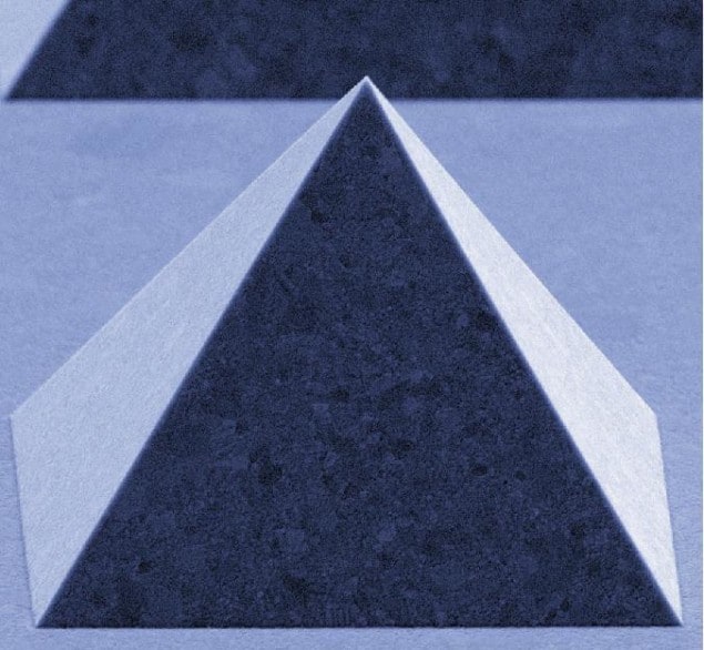
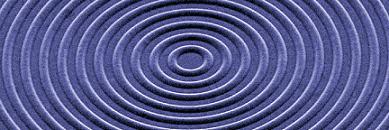
Nagpal and Lindquist made silver bull’s eyes, gold pyramids, triangular grooves and nanohole arrays using this method. “The first time we saw them, we were pretty excited,” Norris said. “They were beautiful.”
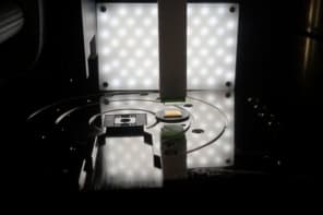
To test how good its surfaces were at conveying plasmons, the team produced a 200 nm thick grooved silver film, and cut slits in it with ion beams. Shining light through these slits from the adhesive side caused plasmons to move across the metal, until they hit the grooves and scattered light.
Measuring the intensity of the scattered light across films with varying distances between grooves allowed Norris and his colleagues to calculate how far plasmons were propagating. They found that their propagation lengths were close to the theoretical maximum. The plasmons travelled for more than 10 µm, far in excess of the 4 and 5 µm lengths recorded in the best previous studies.
Niek van Hulst of the Institute of Photonic Science in Barcelona, Spain, points out that even this improved propagation length demonstrates the fundamental difficulties of trying to achieve long-range plasmon transport. He says that although other groups had already investigated the impact that template stripping can have on plasmons, the Minnesota researchers have made “a nice advance in fabrication methodology”.
Norris’s team will now seek to apply its approach to applications that exploit plasmonics. In particular gold and silver films can be used to improve molecular and biological sensing in a method known as surface-enhanced Raman spectroscopy. “Many groups have demonstrated it,” explained team member Sang-Hyun Oh, “but what’s missing is a reproducible technique. Our method has the chance to address that problem.”
This research appears in the latest edition of Science.


