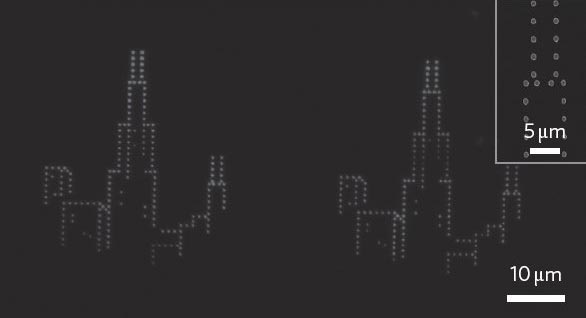
Researchers in the US have invented a new and very fast way of creating nanometre-sized features over large surface areas. The optical nanolithography technique could be used to rapidly prototype miniature devices, such as photomasks, circuits and photonic components. To prove that the technique works, the team used it to “draw” 15,000 identical tiny Chicago skylines.
Scientists are currently developing a variety of lithography techniques for making nanoscale components for integrated circuits, optoelectronics and medical diagnostic devices but most of these methods have inherent disadvantages. For example, “far-field” optical lithography is limited by the so-called diffraction limit of light, which means that it is extremely difficult to create features smaller than several hundred nanometres. Techniques based on “near-field” scanning optical microscopy (NSOM) can overcome the diffraction limit by bringing the light source very near to the surface, but they are low-throughput and can only scan small areas at a time.
The new technique has been developed by Chad Mirkin and colleagues at Northwestern University in Chicago and is called beam pen lithography (BPL). It combines NSOM-based lithography with polymer-pen lithography (PPL), which was also invented and developed by Chad Mirkin, in 2008. PPL uses tiny “pens” made out of polymers to deliver chemical materials to a surface, whereas BPL delivers beams of light to a surface coated with a light-sensitive material.
Array of pyramids
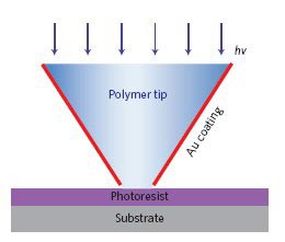
BPL uses an array of around 200 tiny pyramid-shaped pens made from PDMS polymer to create nano- and micro-patterns over areas as large as centimetres squared. Each pen has a square base that measures several tens of microns long, tapering to a pointed tip that is just 60 nm across.
To make the light pens, the researchers began with an array of pyramid-shaped polymer tips that were then coated with a thin layer of gold. Next, they brought the tips into contact with a glass slide coated with PMMA polymer. This step removes the gold layer from the apex of each tip to leave behind an opening that exposes the PDMS inside.
When light is shone onto the underside of the pyramids (which are open as well), the pyramids channel it to the tips and a fine beam of light emerges from the point where the gold was removed. The light pens can then be used to print highly precise patterns onto a silicon substrate pre-coated with a layer of photoresist, for example, by touching the tips to the substrate for 20 seconds or so.
Off and on
One major advantage of the new tips is that their diameters can be varied from 5 to 500 nm. Another advantage is that some pens can be “shut off” while others are “turned on”, allowing different patterns to printed.
As a proof-of-experiment, Mirkin and colleagues drew 15,000 identical Chicago skylines using the technique. Each skyline pattern is made up of 182 dots, each about 500 nm across, which was the size of the pen tip used.
“The NSOM has always been an attractive tool for doing light-based nanolithography but no-one had come up with a functional way of scaling it up until now,” Mirkin told physicsworld.com. “By inventing BPL and using novel opaque pyramid array architectures with exposed transparent tips, we have overcome this problem and created a way to do custom large-area nano- and micro-scale lithography.”
Nice research tool
Zhenan Bao of Stanford University, who was not involved in the work, says, “This technique is quite nice as a research tool. Normally it is difficult to get smaller than 1 µm-sized features in a normal university clean-room unless electron-beam lithography is used but BPL allows one to image small features on the substrate and write patterns on the existing features at high resolution.”
BPL might lead to a sort of “desktop printer” for nanofabrication, adds Mirkin. “Such an instrument would allow researchers to rapidly prototype and possibly produce high-resolution electronic components directly in the lab – without having to send out the test patterns to an outside third-party first, which is what happens now.”
The team now plans to build structures where each pen can be individually addressed using light modulators.
The work is reported in Nature Nanotechnology.
