A new device that combines graphene with special metallic nanostructures could lead to better solar cells and optical communications systems. That is the claim of researchers in the UK who have measured a 20-fold enhancement in the amount of light captured by graphene when it is covered by such nanostructures. The work provides further evidence that the material might be ideal for making photonics and optoelectronics devices, despite the fact that it does not have an electronic bandgap.
Graphene is a sheet of carbon atoms arranged in a honeycomb-like lattice just one atom thick. Since its discovery in 2004, this “wonder material” has continued to amaze scientists with its growing list of unique electronic and mechanical properties. Some believe that graphene could find uses in a number of technological applications – even replacing silicon as the electronic industry’s material of choice. This is because electrons whiz through graphene at extremely high speeds, behaving like “Dirac” particles with no rest mass.
Graphene also shows great promise as a candidate for photonics applications – especially optical communications, where speed is an issue. The material has an ideal “internal quantum efficiency” because almost every photon absorbed by graphene generates an electron-hole pair that could, in principle, be converted into electric current. Thanks to its Dirac electrons, it can also absorb light of any colour and has an extremely fast response to light. The latter suggests that it could be used to create devices that are much faster than any employed in optical telecommunications today.
Drawbacks addressed
Researchers have also already shown that they can make basic solar cells, light-emitting devices, touch screens, photodetectors and mode-lock ultrafast lasers from the material. However, there are, of course, drawbacks: graphene’s “external quantum efficiency” is low – it absorbs less than 3% of the light falling on it. Furthermore, useful electrical current can only be extracted from graphene-based devices that have electrical contacts with an optimized “asymmetry” – something that has proven difficult to achieve.
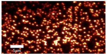
Now, researchers at the University of Cambridge and the University of Manchester may have solved both these problems by pairing up graphene with plasmonic nanostructures. These are metal devices that enhance local electromagnetic fields in a material by coupling incoming light with electrons on the surface of the metal. The nanostructures are fabricated on top of graphene samples to concentrate the electromagnetic field in the region of the material where light is converted to electrical current, so as to dramatically increase the generated photovoltage.
The team, which includes Manchester’s Andre Geim and Kostya Novoselov, winners of the 2010 Nobel Prize for Physics for their discovery of graphene, started out by preparing samples of graphene using the now-famous “sticky tape” method. This involves mechanically shaving off single layers of graphene from a block of graphite. The researchers then made two-terminal electronic devices from the material by forming contacts made of titanium and gold on the graphene using electron-beam lithography. Next, various plasmonic nanostructures were assembled close to the contacts.
Highest efficiency so far
The new devices have an external quantum efficiency of almost 50%, the highest value to date for graphene, says team member Alexander Grigorenko of Manchester. This boosts the light-harvesting capacity of graphene by more than an order of magnitude compared to its non-contacted counterpart, without sacrificing its speed. “If the plasmonic nanostructures we employed were optimized, it should be possible to realize perfect light-to-current conversion, where every photon falling on graphene is converted into current,” he told physicsworld.com. “This is exactly what the solar cell industry is waiting for.”
Furthermore, the problem of creating contacts with the desired asymmetry is addressed through the use of titanium and gold in the device.
“Our work is the first step towards ‘perfect’ photodetectors and solar cells because we have shown that plasmonics helps graphene convert light into electricity with ideal efficiency,” says Andrea Ferrari, who led the Cambridge effort in the collaboration. “Optimizing light interaction and photovoltage generation in graphene will be key for a range of applications, such as solar cells, imaging and telecommunications.”
Profusion of charge carriers
Graphene could also be a viable alternative to conventional plasmonic and nanophotonic materials, he added, because it has many advantages over these materials. It can absorb light over any wavelength in the electromagnetic spectrum from the ultraviolet to visible and far-infrared wavelengths, which means there is no need for bandgap engineering; and it can confine this light into unprecedented small volumes. The profusion of charge carriers in graphene and the fact that researchers can now produce the material in large quantities and over large areas means that it could outperform all existing semiconductor technologies in applications as diverse as photodetectors, tunable ultrafast lasers and imaging, claims Ferrari.
“Graphene seems a natural companion for plasmonics,” adds Grigorenko. “We expected that plasmonic nanostructures could improve the efficiency of graphene-based devices, but did not expect that the improvements could be so dramatic.”
Spurred on by its new results, the team now plans to study how light interacts with graphene in more detail. The researchers also hope to optimize their plasmonic nanostructures, for example by exploiting coupled or “cascaded” plasmon resonances that could further enhance the photovoltage generated. “We might also be able to increase light absorption even more by employing several layers of graphene, something that could lead to a 100-fold enhancement of the photovoltage,” states Ferrari.
The work is published in Nature Communications 10.1038/ncomms1464.