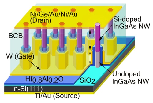
Researchers in Japan have made an important advance in developing a new type of silicon-based transistor by successfully creating vertical transistors from semiconducting nanowires on a silicon substrate. The wires, made from indium gallium arsenide (InGaAs), are surrounded by 3D – rather than planar-shaped – gates, with the finished devices having extremely good electronic properties.
Over time, conventional microelectronic circuits, based on metal–oxide–semiconductor field-effect transistors (MOSFETs), have become ever smaller, and this is one of the main reasons for their success. However, many problems, such as off-state current leakage and the so-called short-channel effect, become more apparent as device size decreases.
To overcome these complications, the gate structure of silicon-based transistors has already gone from being 2D (planar) to 3D with the development of “fin” field-effect transistors (FETs) in the last few years. Researchers are currently looking at planar and fin architectures using compound III–V semiconductors, such as InGaAs, as alternatives to complementary metal–oxide–semiconductors (CMOS) because of their high electron mobility and excellent compatibility with existing gate-dielectric materials. A new “surrounding gate” architecture – whereby the gate is wrapped around a nanowire channel – also shows great promise. However, such structures are difficult to study because it is not easy to integrate freestanding semiconducting nanostructures, such as nanowires, onto silicon substrates.
Nanowire channels
Now, Katsuhiro Tomioka and colleagues at Hokkaido University in Sapporo have developed a new technique to grow vertical InGaAs nanowires. They have shown that it is possible to fabricate surrounding-gate transistors using these wires and core-multishell nanowires – which are made from InGaAs/InP/InAlAs/InGaAs – as channels. The channels have a six-sided structure, which has the benefit of greatly increasing on-state current and device transconductance.
The researchers measured the on–off current ratio in their devices to be about 108 – a value that is superior to that observed in devices made from similar materials with equivalent dimensions. At about 7850 cm2/V·s, the estimated field-effect mobility of the transistors is much higher than the typical electron mobility of a silicon metal–oxide–semiconductor FET. These properties mean that the new devices could be useful as building blocks for high-speed wireless networks and other sophisticated technologies, says Tomioka.
Vertical transistors
“Nature recently published several review papers about new gate architectures, alternative channels and alternative switching mechanisms for future CMOS technologies,” Tomioka explains. “At a recent major conference for transistor researchers, Intel suggested that integrating group III–V material onto silicon could be the future of low-power, high-speed CMOS. The company also emphasized the importance of vertically oriented 3D transistors.”
He adds that the results are “the first to realize these predictions”. The team now plans to fabricate p-type FETs for logic operations using the new technique.
The work is described in Nature.


