Researchers in the US have reported on a new way to increase the amount of light absorbed by thin-film solar-cell materials. The new technique relies on “whispering gallery” modes in which light becomes trapped inside tiny shells made of silicon. The result could lead to more efficient photovoltaics, claims the team.
Nanocrystalline silicon could be ideal for making photovoltaic devices because it is an excellent conductor of electricity and can withstand harsh sunlight without suffering any damage. However, there is a problem: silicon does not absorb light very efficiently. Layers of the material have to be built up to increase the amount of light absorbed – a process that is both time-consuming and expensive.
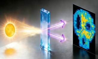
Now, Yi Cui and colleagues at Stanford University have shown that nanoshells made of silicon could offer a quicker and cheaper route to solar-cell fabrication. The cavity inside such a structure confines light in a “whispering gallery” mode, whereby the light orbits around the edge of the cavity at precise resonant frequencies as a result of total internal reflection. “Light effectively gets trapped in these hollow shells,” explains Cui. “It circulates round and round rather than just passing through, and this is very desirable for solar applications because the longer the light is kept in the material, the better its absorption will be.”
Silica balls
The researchers created their nanoshells by first fabricating balls of silica just 50 nm in size and coating these with a layer of silicon. Next, they etched away the glass centre of the shells using hydrofluoric acid. The acid does not attack the surrounding silicon layer and so the technique produces a light-sensitive silicon shell.
The nanoshells can be made in a matter of minutes. In contrast, a micrometre-thick flat film of solid nanocrystalline silicon with equivalent light-absorbing properties would take a few hours to deposit. The nanoshells also absorb light over a broader spectrum than the flat layer of silicon.
And that is not all: a significantly smaller amount of material is required to make a nanoshell compared with a flat silicon slab – roughly 5%, according to Cui and co-workers. This is something that could obviously bring down processing costs. “Looking down the road, the fact that much less material is required to make these nanoshells might come in useful when manufacturing many other types of thin-film cells, such as those that use rarer, more expensive materials like tellurium and indium,” he told physicsworld.com.
New applications
The nanoshells are also fairly indifferent to the angle of incoming sunlight hitting them and the layers are able to bend and twist without becoming damaged. “All these factors might open up an array of new applications in situations where optimal exposure to the angle of the Sun is not always possible,” adds Cui. “Imagine solar sails on the high seas or photovoltaic clothing for mountain climbing, for example.”
Having performed detailed theoretical calculations on the nanoshells, the researchers are now busy making real cells from silica. “We are also exploring the structures to see if they can be used in other types of applications, such as solar fuels and photodetectors as well,” reveals Cui.
The work is described in Nature Communications.