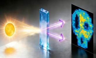
Researchers in Spain have fabricated a new, highly sensitive photodetector from graphene and semiconducting quantum dots. The device is a billion times more sensitive to light than previous graphene-based photodetectors and might be ideal for a variety of applications, including light sensors and solar cells, infrared cameras for night vision and in biomedical imaging.
“In our work, we managed to successfully combine graphene with semiconducting nanocrystals to create complete new functionalities in terms of light sensing and light conversion to electricity,” says Gerasimos Konstantatos, who was co-leader of the team at the Institute of Photonic Sciences (ICFO) in Barcelona. “In particular, we are looking at placing our photodetectors on ultrathin and flexible substrates or integrating the devices into existing computer chips and cameras,” adds co-leader Frank Koppens.
Graphene is a sheet of carbon atoms arranged in a honeycomb-like lattice just one atom thick. The material could find use in a number of technological applications and in the future could even replace silicon as the electronic industry’s material of choice, thanks to its unique properties. These include extremely high electrical conductivity, which comes about because electrons whizz through graphene at extremely high speeds, behaving like “Dirac” particles with no rest mass.
Ideal internal quantum efficiency
Graphene also shows great promise for photonics applications because it has an ideal “internal quantum efficiency” – almost every photon absorbed by the material generates an electron–hole pair that could, in principle, be converted into electric current. Thanks to its “Dirac” electrons, it can also absorb light of any colour.
However, all is not perfect because graphene’s “external quantum efficiency” is low – it absorbs less than 3% of the light falling on it. Another problem is that useful electrical current can only be extracted from graphene-based devices that have electrical contacts with an optimized “asymmetry” – something that has proven difficult to achieve.
Koppens, Konstantatos and colleagues began with a piece of high-quality graphite from which they obtained graphene flakes using the now-famous “Scotch tape” technique. This involves placing the graphite sample on a piece of sticky tape then folding and unfolding the tape a few times until some grey transparent pieces of material can be seen among the original black and shiny fragments of graphite. Next, the researchers press the tape with the transparent graphite onto a substrate and then remove the tape.
“We can see many pieces of graphite with varying thicknesses on the substrate, and look for the ones with the lowest contrast – these are graphene,” explains Koppens. “It is remarkable that we can see a one-atom-thick layer of material with the naked eye, but that is thanks to graphene’s unique interaction with light.”
Hybridizing with quantum dots
The teams then used nanoscale lithography to contact a sample of graphene to two gold electrodes for subsequent electrical measurements. The electrodes are positioned with sub-micron precision in a process whereby gold is evaporated onto a resist mask especially drawn for the flakes with an electron-microscope gun. The next step is to hybridize the graphene with colloidal semiconducting quantum dots that photosensitize the carbon material.
“We chose quantum dots because of their unique optoelectronic properties,” says Konstantatos. The materials can be tuned to absorb a wide range of light wavelengths simply by changing the size of the nanocrystals. They also absorb light very strongly. Moreover, the dots can be processed in solution and can thus be sprayed, spin cast or ink-jet-printed onto any substrate, including graphene, at low temperatures and in air – non-negligible advantages that could bring down costs and simplify fabrication.
The researchers used lead-sulphide quantum dots because the band gap in these semiconductors can be tuned in the technologically important short-wavelength infrared (SWIR) and near-infrared (NIR) ranges.
Tailored connections
“A critical part of our experiment involves ligand exchange to cross-link the quantum dots with short (around 0.2 nm) molecules and attach these to the graphene,” explains Konstantatos. “This step was needed to passivate the surface states in the quantum dots and so allow for efficient charge-carrier transfer to graphene and suppress unwanted recombination of electrons and holes – which would have lowered the amount of current eventually produced by the finished photodetector.” The challenge was to tailor the electrical connections between the semiconducting nanocrystals and graphene while maintaining the high quality and exceptional electrical conductivity of this material, he adds.
After depositing a thin film of the quantum dots on the graphene, the ICFO researchers characterized their device by exposing it to light while probing its resistance at the same time. The photodetector responded to tiny amounts of light (almost complete darkness), as seen by the large change in its resistance.
Since the device was designed in a transistor arrangement, it was possible to change the carrier density in the graphene by varying the voltage on the gate electrode. “From these measurements, we could very precisely quantify the internal quantum efficiency of the device as being greater than 25% because the quantum dots absorb light so well and because charge transfer between the two materials is so effective,” says Koppens. “We found that we could also optimize this performance with the voltage on the gate or even switch off the response. This ‘switchability’ might come in useful for pixelated imaging techniques.”
Bendy solar cells
Many of today’s photonic devices rely on ultra-efficient conversion of light to electricity, Konstantatos adds. “Our detector could be used in digital cameras, for night vision and in biomedical imaging, as well as in sensing applications. Its flexibility also means that it might be ideal for bendy solar cells that could be placed on objects of any shape – an avenue that we are currently exploring.”
The team now plans to scale up the detector to large-scale imaging arrays. “We expect that most cars will be equipped with night-vision systems in the near future and our arrays could form the basis of these,” says Koppens. The researchers also aim to improve their device even further so that it can detect single photons.
The current work is detailed in Nature Nanotechnology.