Researchers in the UK say they have observed behaviour that is very close to an optical version of “Anderson localization” in a mat of gallium-phosphide nanowires – a material that is a strong scatterer of light. As well as shedding light on a fundamental principle of condensed-matter physics, the finding might help make better light-emitting diodes (LEDs) and solar cells, says the team.
Thanks to its wave-like properties, light can produce complex interference patterns when it interacts with materials. For many years, scientists have been trying to produce materials that interact so strongly with light that they modify its flow. Examples of such materials are photonic crystals, which are periodic structures that affect the motion of light in much the same way as crystalline solids affect the flow of electrons.
For disordered structures, random light scattering and interference can produce an effect called localization, in which a light wave becomes “stuck” in closed paths inside the material, bouncing back and forth in complex looping paths called “modes”. Photons cannot easily escape but instead travel around in circles inside the medium.
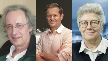
This effect should occur for all types of waves, be they light, sound or the wavefunctions of electrons or atoms. It was predicted in 1958 by Philip Anderson, who bagged the 1977 Nobel Prize for Physics for his discovery. If Anderson localization could be made to occur inside a device that works by absorbing photons (a solar cell, for example), then the cell could be more efficient at converting light into electricity. In LEDs the opposite effect would be seen – photons would build up in the device and lasing would be seen in certain regions as the photons started interacting with each other. This would reduce the threshold for light emission, thereby leading to better LEDs, explains team leader Otto Muskens of the University of Southampton.
Critical threshold
Observing the effects of Anderson localization in real experiments is no easy task, however. In metals, interactions between electrons have so far made it impossible to isolate a distinctive signature of the effect. Researchers have enjoyed more luck studying localization effects in the laboratory using acoustic and matter waves.
Light shows great promise for observing Anderson localization because, unlike electrons, photons do not interact significantly with each other; however, there are challenges. “For light waves in 3D materials, we can only analyse the light that ‘leaks out’ of a material,” says Muskens, “but in our new experiments we have clearly seen some of the predicted interference patterns near a so-called critical threshold for Anderson localization. Such observations are exciting in themselves because they show that we are very close to seeing the real Anderson-localization regime.”
The Southampton team studied a mat of gallium phosphide (GaP) semiconductor nanowires, made with the help of colleagues at the University of Eindhoven and Philips Research Laboratories in Germany. GaP is one of the strongest 3D light-scattering materials known and the researchers were able to convert a coherent laser beam into random light by passing the beam through the nanowire structure.
Strongly correlated transport
“By using methods from statistical optics, we were able to show that the laser light becomes ‘grainy’ after passing through the GaP mat,” Muskens explains. “We collected several thousand different snapshots of these grainy light patterns leaking out of different places on the sample, something that allowed us to compare our results with theoretical predictions.”
It turns out that the light transported through the nanowires does not become completely random but still remains strongly correlated. Light waves interact inside the nanostructure thanks to an effect called mesoscopic interference. Such strongly correlated transport invalidates conventional light-diffusion models for describing photon transport and emission in certain nanostructures, like these light-scattering nanowire mats, says Muskens.
“More is different”
In this experiment, mesoscopic refers to a length scale between that of the individual nanowires and the macroscopic scale of the sample, Muskens explains. “In practice, mesoscopic effects become important on a scale of 10–100 times the diameter of the nanowires, but it is important for us to be able to distinguish collective effects from the effects caused by single nanowires,” he says. “Anderson himself once said that ‘more is different’ (the title of one of his papers), implying that when you increase the complexity and scale of a system, new physics will emerge. It is not just the simple sum of the individual building blocks (nanowires in our case) that is important, but how the blocks are arranged. A good example of this principle is high-temperature superconductivity, but in photonics an emergent phenomenon is wave localization.”
Because arrays of nanowires are increasingly being used in technologies such as LEDs and solar cells, such mesoscopic effects might be exploited to improve these applications. “It is particularly tempting to think about how increased light trapping might enhance nanowire photovoltaics. For example, the effect of trapped light travelling in circles could be used to increase light absorption in thin-film devices. We might even be able to improve LED performance by coupling to the light looping modes, but much more research is still needed before we can say this with any certainty,” says Muskens.
The current work is published in Nature Photonics.


