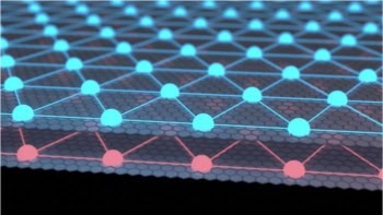
Researchers at the Massachusetts Institute of Technology in the US have developed a new way to p-dope graphene that does not sacrifice its excellent electronic properties too much – something that has proved to be a challenge until now. The resulting material could be ideal for making all-graphene integrated circuits on a chip, radio-frequency transistors and nanoelectronic circuit interconnects to name a few examples.
Graphene is a flat sheet of carbon just one atom thick – with the carbon atoms arranged in a honeycombed lattice. Since the material was first isolated in 2004, its unique electronic and mechanical properties – which include extremely high mobility and high strength – have amazed researchers, who say that it could be used in a host of device applications. Indeed, graphene might even replace silicon as the electronic material of choice in the future, according to some. This is because electrons can whizz through graphene at extremely high speeds, behaving like “Dirac” particles with no rest mass – a property that could allow for transistors that are faster than any existing today.
However, unlike the semiconductor silicon, graphene has no gap between its valence and conduction bands. Such a band gap is essential for electronics applications because it allows the flow of electrons in the material to be switched on and off. One way of introducing a band gap into graphene is to chemically dope it, but this has to be done carefully so as not to destroy the material’s unique electronic properties.
Plasma-based surface-functionalization technique
A team led by Mildred Dresselhaus and Tomas Palacios has now succeeded in p-doping graphene with chlorine using a plasma-based surface-functionalization technique. “Compared with other chemical-doping methods, the advantages of our approach are very significant,” says team member Xu Zhang. “First and foremost, the chlorine-doped graphene keeps a high charge mobility of about 1500 cm2/Vs after the doping. This value is impressively high compared with those obtained with other chemical species previously.”
The chlorine can also cover more than 45% of the surface of the graphene sample, he adds. This is the highest surface-coverage area reported for any graphene doping material until now, according to the researchers.
Density-functional theory predicts that a band gap of up to 1.2 eV can be opened up in graphene if both sides of the sample are chlorinated and if the amount of chlorine on each side covers 50% of the total sample area. “The 45.3% coverage in single-sided chlorinated graphene observed in our work is thus important and paves the way to ultimately opening up a sizable band gap in the material while maintaining a reasonably high mobility,” Zhang told physicsworld.com.
In their work, the researchers studied both “exfoliated” graphene and that obtained using chemical-vapour deposition (CVD). They performed the chlorine-plasma treatments in an electron cyclotron resonance reactive ion etcher (ECR/RIE) in which chlorine gas was excited into the plasma state by absorbing energy from an in-phase electromagnetic field at a certain frequency. The chlorine plasma was accelerated by applying a DC bias relative to the sample stage. “We carefully optimized both the ECR power and DC bias to control the reaction conditions,” explains Zhang, “and the experiments were performed at room temperature.”
The p-doped material produced could be used to make all-graphene integrated circuits on a chip and radio-frequency transistors, he adds. Doping the graphene with chlorine also reduces its sheet resistance, making it suitable for use in electronic-circuit interconnects.
The team now plans to dope suspended samples of graphene with chlorine – to access both sides of a sample – and so open up an even bigger electronic band gap.
The current work is detailed in ACS Nano.


