Picking up a tiny flake of material just one atom thick and placing it with precision onto a substrate is no easy task. But now it has become a bit easier, thanks to researchers at the Kavli Institute of Nanoscience in the Netherlands who have come up with the first all-dry technique for transferring 2D materials such as graphene and molybdenum sulphide.
The new method is said to be quick, efficient and clean, and makes use of viscoelastic stamps. As well as being much simpler than traditional wet-transfer techniques, it could also be used to fabricate freely suspended 2D structures because the samples are not subject to any capillary forces during the process.
2D materials are creating a flurry of interest in labs around the world because they have dramatically different electronic and mechanical properties from their 3D counterparts. This means that they could find use in a host of practical devices such as low-power electronics circuits, low-cost or flexible displays, sensors and even flexible electronics that can be coated onto a variety of surfaces.
Contamination and collapse
The two most famous 2D materials are graphene – a sheet of carbon just one atom thick – and the transition metal dichalcogenides, which include molybdenum disulphide (MoS2). For real-world applications, such materials need to be transferred onto substrates to make “heterostructures” based on the stacking of 2D layers. Most techniques involve wet chemistry, and the chemicals employed often contaminate the 2D materials and adversely affect their pristine electronic and physical properties. Moreover, the capillary forces between the chemicals and the material being transferred can cause the 2D structure to simply collapse.
An all-dry technique could be a solution to these problems, and now a team led by Herre van der Zant and Gary Steele has created just that. The process begins by using the famous “Scotch tape technique”, whereby 2D flakes are peeled off a parent 3D crystal using adhesive film. These layers are then attached to a thin layer of a commercially available viscoelastic material called Gelfilm, which acts as a stamp.
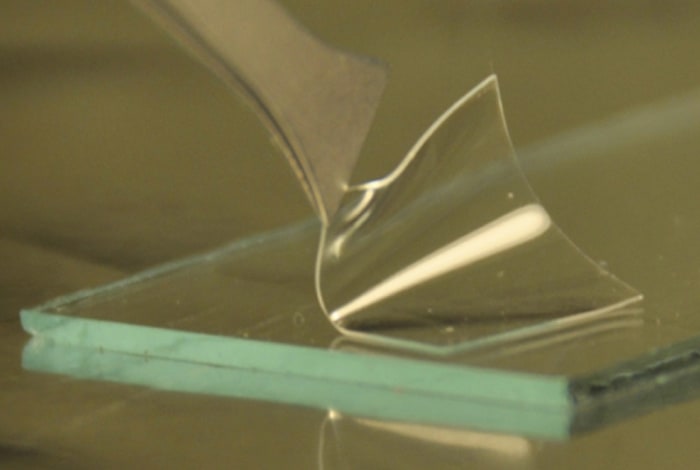
“As the stamp is transparent, we can see the sample through it and can align the flake wherever we want on a 2D substrate surface with sub-micron resolution,” explains team member Andres Castellanos-Gomez. “To transfer the flake, we press the stamp against the sample surface and peel it off very slowly.” The whole process takes just 15 minutes or less.
Climbing toys
The transfer process works thanks to Gelfilm’s viscoelasticity: the material behaves like an elastic solid over short time periods but can flow like a viscous fluid over longer timescales. Such materials are also used to make toys that “climb” down smooth surfaces such as a window by releasing their grip and then re-attaching at a lower point.
The team has already shown that the technique works by transferring graphene flakes onto hexagonal boron nitride (h-BN) – which is a 2D material that is a good substrate for graphene. Using an optical microscope, the researchers were able to confirm that nearly half of the graphene flakes lie flat on the boron nitride without any bubbles or wrinkles.
“Our technique could be applied to any kind of exfoliated layered crystal, so allowing for an infinite combination of material heterostructures,” says Castellanos-Gomez. “For example, as well as depositing graphene on h-BN, we have also already managed to ‘sandwich’ a MoS2 bilayer between two h-BN flakes.”
Beating drumheads
The Kavli team has also succeeded in transferring a single-layer MoS2 crystal onto a silicon oxide/silicon substrate pre-patterned with holes of different diameters. The single-layer MoS2 is freely suspended over the holes, forming “drumheads” – which might be used in mechanical-resonator applications. Indeed, the technique might also be employed to transfer 2D crystals onto pre-fabricated devices with trenches and electrodes.
And that is not all. Since the stamping technique is so gentle, it can be used to deposit 2D crystals onto even the most fragile of substrates. For example, the team says that it has succeeded in transferring few-layer MoS2 crystals onto the cantilever of an atomic force microscope without damaging the cantilever. “We have also transferred 2D materials onto silicon-nitride membranes and holey carbon films, which are typically employed in transmission electron microscopy,” says Castellanos-Gomez.
Details of the new stamping technique can be found in 2D Materials, a new journal from IOP Publishing that publishes its first papers this month.
- There is much more about how to make graphene in this video filmed at the University of Manchester:
This article first appeared on nanotechweb.org.