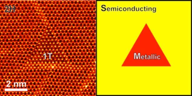
Researchers in Japan say they have watched individual atoms rearrange themselves during the semiconductor-to-metal phase transition in molybdenite (MoS2) – a graphene-like material that can occur in sheets just one molecule thick. Until now, such phase transitions were thought of as collective motions of atoms, but the new observations show that atom-by-atom movements are at play. The result could provide important information to researchers trying to create electronic devices from single sheets of MoS2.
Molybdenite is a direct bandgap 2D semiconductor that shows some promise for use in electronics and optoelectronics devices. The mobility of its electric charge carriers is greater than 100 cm2/Vs (and could be as high as 500 cm2/Vs) – values that compare well to silicon. It is a “van der Waals solid”, which means that it comprises robust 2D sheets weakly bonded to each other to form a layered 3D structure much like graphite. This means that molybdenite is stable on a variety of substrates – even transparent or plastic ones. Single-layer molybdenite is only about 0.65 nm thick, which means that it can be used to create very thin transistors.
An important property of molybdenite is polymorphism: it has different electronic characteristics depending on the crystal structure of the layers. It is a semiconductor when the sulphur and molybdenum are arranged in a trigonal prismatic structure and it is a metal when the atoms assume an octahedral structure. Both structural phases can be thought of as a central plane of molybdenum atoms sandwiched between two planes of sulphur atoms. Phase transitions were believed to occur when the planes glided over each other – but such a transformation had never been directly observed in an experiment until now.
Gliding atoms
Now, a team led by Kazu Suenaga at the National Institute of Advanced Industrial Science and Technology (AIST) in Tsukuba has shown that gliding atomic planes in molybdenite cause a new phase to nucleate in the material. Using a scanning transmission electron microscope (STEM), the group has also spotted intermediate phases that occur during the transition.
The transition process can be triggered by the heat from the STEM electron beam. The electron-beam irradiation introduces a very small metallic domain in the semiconductor phase, which kick-starts the phase transition, explains Sureaga. This process could be used as a controllable way to induce phase transitions in molybdenite and similar ultrathin materials.
“Our result implies that electronic devices, such as nanodiodes, might be made ‘in-layer’ rather than via layer-by-layer bottom-up assembly of layers with distinct properties, which is the conventional way of going about such fabrication,” says Sureaga. “Making nanodevices using bottom-up processes is no easy task, but we show here that simple electron-beam patterning can introduce nanoscale domains with distinct metallic electronic properties within a single-layer semiconducting matrix. We can make the structures with atomic-scale precision and even monitor how the device grows in situ, thanks to observations in the STEM.”
Tiny metal triangle
Indeed, the researchers say that they have already produced prototypes of several nanodevices using their technique. For example, they made a serial junction of semiconductor and metal phases, which is to all intents and purposes a Schottky diode. They also managed to produce a local semiconductor region sandwiched between two metallic electrodes to form a nanoscale transistor. They have also created a tiny triangular-shaped region of metal within a semiconductor sheet of molybdenite (see image above) that can function as a quantum dot.
The research is described in Nature Nanotechnology 10.1038/nnano.2014.64.
- This article first appeared on nanotechweb.org.


