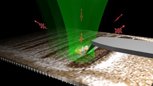
Researchers in France have discovered a new way to image magnetic domain walls on the nanoscale in ultrathin ferromagnetic films – something that has been difficult to do until now. Using a point-like defect in diamond attached to a scanning atomic force microscope (AFM), they were able to map out the energy “landscape” for a domain wall and could even make the walls themselves move using the laser light from the microscope. The technique could help in the development of sophisticated spintronics devices such as racetrack memory.
Magnetic domain walls are narrow boundaries (about 10 to 100 nm in size) between regions in a material where the magnetic moments point “up” on one side of the wall and “down” on the other. At these boundaries, the magnetic moments do not rotate abruptly from one orientation to the other – rather, they shift gradually over the region. When these walls move through a material, they behave rather like a taut elastic band sliding over a rough surface. How they move depends on the potential energy landscape they encounter – energy troughs offer little resistance, but energy peaks act like barriers that are more difficult to overcome.
Magnetic domain walls could be used to make new types of spintronics devices, such as racetrack memories in which data are stored as a sequence of magnetic domains along a nanowire. Individual bits are stored and retrieved by moving the sequence along the nanowire and across magnetic read and write devices. A typical racetrack chip would contain arrays of nanowires a few microns long and about 30 nm wide, and could store hundreds of gigabytes of data. In such devices, researchers would need to precisely control the position of a domain wall, as well as be able to move it along a nanostructure at will. Being able to characterize the magnetic “terrain” for these domain walls would be an important step in this direction, but this has proved difficult to do up to now, for lack of the right tools.
NV microscope
Vincent Jacques and colleagues at the ENS Cachan, the French National Centre for Scientific Research (CNRS) and Université Paris-Sud have now succeeded not only in imaging domain walls, they have also managed to observe the walls jumping along different pinning sites along a thin ferromagnetic wire. They were able to do this using a highly sensitive scanning magnetic microscope based on lattice imperfections known as nitrogen-vacancy (NV) centres in diamond. These defects occur when two neighbouring carbon atoms in the diamond are replaced by a nitrogen atom and an empty lattice site. Such NV sites are capable of detecting weak magnetic fields.
The instrument employed by Jacques’ team actually consists of a 50-nm-sized diamond gem attached to the cantilever of the AFM. When stimulated with green laser light with an external radiofrequency field, the NV centre in the diamond emits light in the red part of the electromagnetic spectrum. The intensity of this light depends on the local magnetic field of the sample being imaged (in this case a 1-nm-thick CoFeB ferromagnetic nanowire).
“By detecting the NV defect emission with the optical microscope, we can precisely determine the magnetic field emanating from the magnetic film beneath the diamond tip,” explains Jacques. “As we move the diamond sensor across the film, we can image the stray magnetic field from the nanowire and determine its domain-wall profile.”
Dragging domain walls
Using their technique, the researchers were also able to observe domain-wall hopping (known as Barkhausen jumps) between two pinning sites spaced 50 nm apart along the wire. Pinning sites come about because of the presence of structural or fabrication defects in a material. They locally modify the energy landscape and hinder the movement the domain walls. They managed to control these jumps using the heat generated by the laser light in the microscope, which in turn allowed them to “drag” the domain wall along the wire and position it at any point on the structure.
“Our process allows us to calculate the energy landscape ‘seen’ by the domain wall along the wire,” says Jacques. “Such a quantitative understanding of this landscape could be important for future applications in data storage and information processing. For example, the racetrack memory device proposed by IBM involves storing bits of data with a sequence of domain walls that are shuttled back and forth along a magnetic wire (the track). As mentioned, a crucial step towards making these memories will involve characterizing the magnetic terrain for these domain walls, because how they move across the track will determine how well they actually perform as devices.” The technique is not just limited to studying domain walls either, he added. “It can also be used to study other magnetic objects, such as skyrmions (tiny magnetic vortices that could form the basis of future hard-disk technologies) – another subject of intense research at present.”
The technique is published in Science.
- This article first appeared on nanotechweb.org


