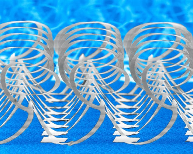
“Tilted table”, “peacock” and “triple-floor building” are just three of many fantastical 3D structures that have been created by compressing simple 2D patterns. The new technique for creating these objects is called compressive buckling, and has been developed by researchers in the US, China and South Korea. The method can be used to create objects with features as small as 100 nm that the team says could be useful for developing new technologies for medicine, energy storage and even brain-like electronic networks.
The ability to produce precision 3D structures on the micrometre or nanometre scale is becoming increasingly important to those developing a range of new technologies. However, the number of techniques currently available is limited. One option is to extend existing methods of manufacturing 2D (or extremely thin 3D) nanoscale structures such as computer chips to allow the creation of true 3D objects. This has proved to be difficult and time-consuming because it involves creating a series of aligned 2D layers on top of one another. Other techniques such as 3D printing, in which fluid nozzles deposit the required shape, lack precision and can be used only for materials that can be deposited as inks.
Silicon challenge
“They are highly constrained in the materials,” explains John Rogers of the University of Illinois at Urbana-Champaign, who is part of the compressive-buckling development team. “You can’t do it with silicon, for example, so there goes all of electronics,” he adds.
One alternative is to make a 2D shape and then apply mechanical forces to transform it into 3D. An established technique called “residual stress-induced bending” uses the stress between layers of two different materials on a 2D surface to cause etched objects to rotate out of the plane. This has been used to tilt micro-mirrors away from a surface, for example.
Now, Rogers and colleagues from the University of Illinois at Urbana-Champaign, Northwestern University, Zhejiang University, East China University of Science and Technology and Hanyang University have created a new 2D-to-3D fabrication technique. The first step is to use computer models to design 2D shapes that, when compressed at specific points held fixed to a surface, will relieve the applied compressive stress by buckling into desired 2D structures. The next step is to etch these 2D precursor shapes onto a silicon wafer and then chemically modify the points that must stay fixed when compressed. The pattern is then transferred onto a sheet of stretched silicone rubber. When the silicone rubber relaxes to its natural shape, the silicon precursor is compressed. The points on the silicon that had been chemically modified form chemical bonds to the silicone rubber and stay fixed, while the other points buckle upwards.
Creating design tools
Using this type of controlled buckling, the team managed to produce a variety of elaborate 3D shapes. The researchers even produced structures with multiple levels of elevation by designing shapes in which the relief of stress in the initial 2D shape would create further buckling, raising another part of the shape further. “We have senior co-authors on this paper who have developed really quantitatively precise models of how the mechanics works,” says Rogers. “We are just beginning to explore those models as design tools to investigate what range of topologies we can access in this way.”
Vladimir Aksyuk of the National Institute of Standards and Technology in Boulder, Colorado, commends the work. “This is interesting because it shows that, without having a built-in bilayer or residual stress gradient, you can go from purely planar to a diversity of shapes. That’s somewhat surprising to me,” he says. Vladimir Tsukruk of the Georgia Institute of Technology agrees, describing the variety of shapes demonstrated as “amazing” and the prospective applications of the technique as “astounding in breadth and impact”. This, he says, will be one of the key future challenges: to demonstrate that the technique can genuinely be used to make something that cannot be produced using a method currently in use or do it much more simply than before.
The team is now focusing its attention on these areas. Rogers looks forward to “an electronic cell or tissue scaffold”. “A lot of the people that we talk to are enthusiastic about what you can do when you go from a passive scaffold to something that embeds full electronic functionality,” he says. Rogers claims that this would allow researchers to produce “high-performance electronic networks in configurations that resemble the 3D networks that exist in the brain or the vasculature that provides blood flow to the heart”.
The research is published in Science.


