A stretchable and bendable transistor has been made by researchers in the US by applying the principles of kirigami – the Japanese art of paper cutting – to graphene. The researchers have also made tiny graphene-based hinges and pyramids, and they are confident that they could reduce the size of their devices to the nanometre scale. The team also points out that the current micro-scale devices could be useful for biocompatible electronics, including probes for the study of neurons.
The mainstay of the electronics industry, silicon, is rigid and brittle, and is therefore not appropriate for making deformable electronics. The ability to deform is particularly useful for electronic devices that interface with biological organisms, for example sensitive prosthetic skin and subcutaneous sensors, which must bend and stretch with surrounding tissue. Graphene is a flexible sheet of carbon just one atom thick, and could offer a way to create deformable electronics because of its high electrical conductivity. One problem with graphene, however, is that it stretches very little.
Nanoscientist Paul McEuen and colleagues at Cornell University in Ithaca, New York, were inspired to try graphene kirigami after they investigated the bending stiffness of the material. They used an infrared laser beam to press on a gold pad located on the tip of a graphene cantilever that is about 10 μm long. By measuring the displacement in response to the known force of the laser photons, they calculated the bending stiffness of the material. They also monitored the thermal oscillations of a graphene cantilever and calculated the stiffness from the oscillation amplitude.
Like crumpled paper
Curiously, both measurements showed that graphene was about 4000 times stiffer than theoretical calculations predict. The reason appears to be that free sheets of graphene contain ripples, both from thermal fluctuations of the carbon atoms and manufacturing imperfections that arise when it is delaminated from a substrate. These cause monolayer graphene to behave like crumpled paper, which is much harder to bend than pristine paper.
While this might seem like a strike against the possibility of graphene-based deformable electronics, McEuen points out that the ratio of graphene’s bending stiffness to its stretching stiffness is no greater than that of paper, and both values are orders of magnitude lower. This, he says, makes the material suitable for the ancient Japanese art of kirigami. This involves making strategic cuts in paper so that the material can bend and stretch in much the same way as bending a metal wire into a spring allows the resulting structure to stretch.
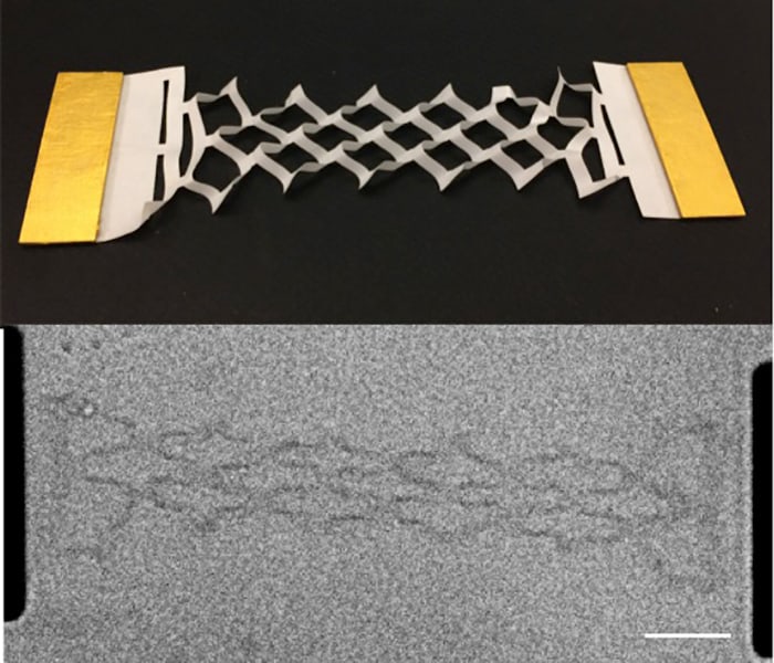
McEuen and colleagues created their kirigami structures by first depositing tiny gold pads onto graphene sheets and then used lithography techniques to create patterned networks of kirigami cuts. They used this cut graphene to create electrolyte-gated transistors, and found that the electrical properties of these transistors were virtually unchanged, even when the transistors were stretched to 240% of their original length. Although the transistors were only one atom thick, they could be stretched and contracted more than 1000 times without degrading their electrical properties.
Gold-peaked pyramid
The team also produced graphene hinges that connected two pads together to create door-like devices. The devices were designed to be opened and closed either mechanically or magnetically, and survived about 10,000 open/close cycles before the gold pads started to warp. Perhaps the most eye-catching device created by the team is a pyramid-like structure with a gold peak that can be raised more than 10 μm above the graphene surface using the force of a laser beam (see figure above).
McEuen says the researchers worked at the micron scale partly for experimental convenience, but adds that there is nothing stopping them from further miniaturizing the devices to the nanometre scale. “All of the experiments were done in water using an optical microscope,” he explains, “If we went to the nanometre scale we wouldn’t be able to see anything.”
The current size of the devices is approximately the same size as many living cells, and this makes the technology ideal for many of the biological processes studied by McEuen’s team. “If you’re trying to detect the signal from a neuron, probably the 10 μm scale is the size that you would want. If you’re trying to make a device that can fold up and go inside a cell and then release some drug or chemical, you might want to make it much, much smaller, so it would have a better chance of being brought across the cell membrane.”
Nanoscientist Nicholas Kotov of the University of Michigan, whose own group recently published similar work using electrically conductive paper composites instead of graphene, is impressed by the researchers’ demonstration of “the applicability of the kirigami approach to the micron scale and to very thin sheets”. However, he points out that composites are better materials to work with at larger sizes.
Christian Santangelo of the University of Massachusetts, Amherst, agrees the work is “pretty exciting”, and thinks that the very fact that this can be done with graphene will interest researchers working to exploit the novel electrical phenomena of the material, although he thinks a quantitative, predictive model of the unexpected bending stiffness of graphene would also be an important contribution to our knowledge of the material.
The devices are described in Nature.