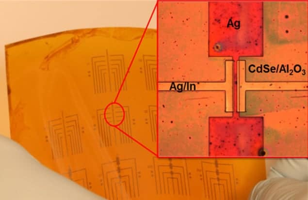
A high-quality, flexible transistor, made entirely from colloidal nanocrystals, has been developed by a team in the US. By sequentially depositing their components in the form of nanocrystal “inks,” the researchers could make transistors using standard industrial methods, without the need for high-temperature, high-vacuum specialist equipment. The work can be scaled up, so it could be applied to a variety of materials, and even in the design of printable circuits for wearable or implantable electronic devices.
The transistor has been the central component of the electronics industry since its Nobel-prize-winning invention by John Bardeen, Walter Brittain and William Shockley in 1948. Modern CMOS (complementary metal-oxide semiconductor) computer chips contain billions of transistors etched into a single, high-purity silicon wafer. However, scientists and engineers are now keen to incorporate electronic devices into ever-more unlikely places: from wearable displays on clothes to implantable glucose monitors. Many of these applications demand flexible devices, whereas crystalline silicon is inherently brittle.
Flexible crystals
Electrical engineer Cherie Kagan and colleagues at the University of Pennsylvania have been part of a worldwide effort exploring the potential of colloidal nanocrystals to create flexible transistors and other electronic components. “In the past, we’ve shown that you can make conductive wiring using silver nanocrystals,” says Kagan. “We’ve also shown that we could use semiconductor nanocrystals, or quantum dots, to make good semiconductor layers.” However, to create transistors, they had to turn to conventional techniques of high-performance computing to deposit the source, gate and drain connections, as well as the insulating layer, by vacuum evaporation. Kagan told physicsworld.com that because fabrication facilities are very expensive, “simple printing- and coating-based methods” are attractive – especially for applications that require devices over large areas.
Now, Kagan’s team has created the first transistor built entirely from various types of nanocrystals. The researchers first deposited a layer of conductive silver nanocrystals from solution on a flexible polymer, using a photoresist to define the position of the electrode. After removing the photoresist, they deposited a layer of insulating aluminium-oxide nanoparticles from another solution, surrounding the gate electrode. On top of this, they deposited cadmium-selenide quantum dots – these act as the transistor’s semiconductor channel. Finally, the researchers patterned more silver nanocrystals on top to act as the source and drain leads. Mixing indium nanocrystals with the silver of the source and drain leads and heating the devices to 250 °C after manufacture allowed the researchers to dope the semiconductor channel with metal ions (n-doping), as the indium diffused from the silver leads into the cadmium selenide.
An electric field was created by raising the electrical potential of the gate electrode, thereby attracting electrons into the semiconductor, increasing its electrical conductivity and allowing current to flow between the source and drain electrodes. This allowed the device to behave as a field-effect transistor (FET) – the most industrially popular type of transistor used today. Upon testing, the team found that its devices functioned as well as state-of-the-art FETs produced by vacuum evaporation.
Looking forward
“The next step would be to exploit what we’ve demonstrated and to develop some of the 3D-printing-based techniques for additive manufacturing. That’s the one that excites us the most as we think about how you would be able to connect these different layers on your substrate to make integrated circuits.” But Kagan also points out that, for standard CMOS logic architectures, they would need to develop a p-type transistor, in which conductivity occurs via positive “holes” and raising the gate potential turns off the transistor. Dmitri Talapin, from the University of Chicago, who was not a part of Kagan’s team, suggests a potential solution for this, saying that “future printable circuits will combine p-type organic transistors with n-type nanocrystal devices to enable CMOS device architecture. The work of the Kagan group represents an important milestone on this way.”
Nanocrystals expert Maksym Kovalenko of ETH Zurich in Switzerland, who was not involved in the current work, describes the research as remarkable, adding that it shows the “level of maturity in this field”, now that it is possible to make nanoparticles, as well as tune their properties. “I think this shows very clearly that you can make any major optoelectronic device fully out of nanoparticles,” he adds.
The research is published in Science.


