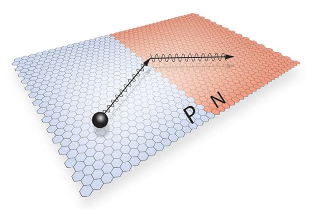
The negative refraction of electrons in graphene has been seen for the first time in experiments done by physicists in the US. The work represents an important advance in the fabrication of graphene electronic devices, and could lead to new applications of graphene such as low-power transistors.
Negative refraction can occur when light or other waves cross an interface between two different materials. The term “negative” is used when the direction of the light is bent in the opposite direction to that which occurs for conventional materials such as glass and water. Negative refraction is a property of some artificial metamaterials and can be used to bring diverging rays back to a focus – allowing for the creation of a perfect lens. First proposed by the Russian physicist Victor Veselago in 1968, various types of negative refraction materials have subsequently been produced and the concept has been applied to the design of invisibility cloaks. However, actually making practical metamaterials has proven to be very difficult.
In principle, it should be much easier to achieve negative refraction with electron waves in a semiconductor. For electrons in a solid, the equivalent quantity to the optical index of refraction is the Fermi wave vector. This intrinsic property points in the same direction as the electron flow in an n-type semiconductor – in which charge is carried by electron flow. In a p-type semiconductor, however, charge is carried by positive “holes” and the wave vector points in the opposite direction. At the interface between an n-type and a p-type semiconductor (a “p–n junction”), the Fermi wave vector therefore changes sign and negative refraction should result.
Too much reflection
In practice, however, no one has been able observe negative refraction at a p–n junction. The main reason is that in conventional semiconductors with an energy gap between the valence and conduction bands, an electron has to gain or lose energy to traverse a p–n junction. The result is that the vast majority of electrons are reflected at the junction rather than being transmitted across and therefore refracted.
Graphene is a sheet of carbon just one-atom thick and it has no band gap. Therefore p–n junctions made from graphene should be much more transparent to electrons than those made from other semiconductors. Nevertheless, previous attempts to see negative refraction in graphene have failed. In search of an explanation for this failure, Cory Dean of Columbia University and colleagues modelled electron transmission across the p–n boundary in graphene. They concluded the likely culprit was the atomic-scale roughness at the interface that is the result of conventional lithographic processes used to make the junctions.
“Say you shine a focused laser beam onto a piece of glass, you can see that it refracts and measure the change of direction quite easily,” explains Dean. “Now imagine that you take a piece of sandpaper and scuff the surface of the glass, the beam will get dispersed.”
Flaky solution
To get around this problem, the team fashioned a junction using the natural edge of a graphene flake. They attached multiple electrodes to both sides of the junction. By injecting the electrons on one side and placing the junction in a variable transverse magnetic field, they controlled the angle at which electrons approached the boundary. They then used the voltage on the electrodes on the other side to work out where the electrons had ended up after crossing the junction. By comparing their measurements with computer models, they obtained clear evidence of negative refraction.
The team believes that its findings could lead to several practical applications. Dean says that, in principle, the ability to bring a diverging electron beam back to a focus at one of two points could form the basis of an electronic switch. Such a switch could be operated using very small amounts of energy, and this could be used to boost the efficiency of electronic devices. Dean also suggests that some of the parallels with optical applications of negative-refraction materials – such as cloaking – could be exploited in practical devices: “I don’t think it’s too crazy to think that we could apply some of those same concepts to electrical devices in ways that just haven’t been thought about because the technology just hasn’t been there,” he says.
Theoretical Physicist Carlo Beenakker of Leiden University in the Netherlands is impressed by the work: “The big technical advance is that they’ve been able to make very thin, very abrupt p–n junctions,” he says. “That, by itself, could have very far reaching implications because we know p–n junctions have all kinds of electronics applications.” He is more sceptical about the usefulness of perfect lensing with electrons: “If you have an electronic device, you have a big ohmic contact and shoot in electrons from all directions, and they come out with all directions at the other side,” he says. “We don’t use angular resolution in semiconductor devices, probably because it’s not a robust way to operate a device.”
The research is described in Science.


