Electronic devices that exploit the spin of electrons as well as their charge are poised to overcome a major hurdle that could signal the beginning of an electronics revolution.

Nearly all electronic and optoelectronic devices are made of semiconductors and rely on the exact control of electric charges. Electrons, however, possess a well defined “spin” angular momentum, in addition to a well defined charge. Their spin is either +1/2 or -1/2: in other words an electron can rotate either clockwise or anticlockwise around its own axis with constant frequency. The two possible spin states naturally represent the “0” and “1” states in logical operations. The ability to exploit this spin in semiconductors promises new logic devices with enhanced functionality, higher speed and reduced power consumption – and might spark a revolution in the semiconductor industry.
So far the problem of injecting electrons with a controlled spin direction has held up the realization of such “spintronic” devices. Two recent experiments represent an important step towards electrical spin injection at room temperature. In the first, Klaus Ploog and co-workers at the Paul Drude Institute in Berlin have demonstrated that room-temperature spin injection is possible (H J Zhu et al. 2001 Phys. Rev. Lett. 87 016601). Meanwhile Vincent LaBella and co-workers at the University of Arkansas in the US have shown that the quality of semiconductor surfaces plays a vital role in spin injection (V LaBella et al. 2001 Science 292 1518).
Putting the spin into spintronics
For decades spin-polarized electrons have been created in semiconductors simply by illuminating the material with circularly polarized light. However, electrical spintronic devices should not have to rely on optics. A purely electrical method for injecting spin-polarized electrons into semiconductors is needed to guarantee the success of spintronics – and has provided a surprisingly difficult challenge.
So far, two different concepts have been employed to solve the problem. The first approach involves injecting spins from a dilute magnetic semiconductor that acts as an efficient spin aligner when an external magnetic field is applied. This concept works well at low temperatures – almost all the electrically injected electrons have their spins pointing in the same direction. However, it is extremely difficult to implement at room temperature because most of the known magnetic semiconductors lose their spin-aligning characteristics just above liquid-helium temperatures (i.e. above 4 K).
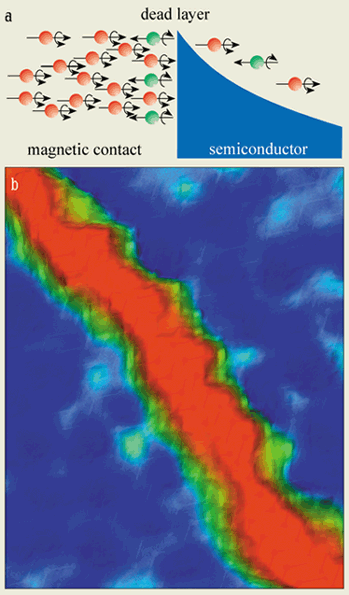
The second approach involves injecting spin-polarized electrons from a ferromagnetic material, where almost all of the conducting electrons are intrinsically aligned. However, this approach also faces problems. Randomly oriented spins – known as magnetically dead layers – in the ferromagnetic material close to the semiconductor interface are a barrier to effective spin injection (see figure a). What is more, theoretical work predicts that spin injection from metals into semiconductors should be virtually impossible. Now an exciting experiment proves the opposite. Ploog and co-workers have demonstrated experimentally that it is possible to inject spin-polarized electrons from iron into gallium arsenide at room temperature.
To get round the problem of spin detection, Ploog and co-workers used a well known trick to prove the existence of polarized electrons. The polarized electrons from the iron were injected into a semiconductor light-emitting device, where they recombined with holes. By measuring the degree of circular polarization of the subsequently emitted light, the Berlin team obtained a direct measure of the spin polarization. The experiment yielded light polarizations of 2% at 25 K and 300 K, which is a good indication that the efficiency of the electron spin injection is much larger at room temperature. Indeed, the injection efficiency must be considerably larger than 2% since the spin lifetime (i.e. the length of time that the electron spin remains aligned in the same direction) in this material is much shorter than the radiative lifetime at room temperature. In other words, the injected spin polarization is partially lost in the semiconductor before the electron recombines with a hole.
Ploog and co-workers also explained the underlying mechanism in terms of a tunnelling process. They argue that the iron and gallium arsenide form a so-called Schottky barrier, a potential barrier that allows electrons to tunnel from one material to the other. This tunnelling process enhances the spin-injection efficiency by reducing the resistance mismatch between the iron and the gallium arsenide – a major obstacle for spin injection according to calculations by Georg Schmidt of the University of Würzburg in Germany and co-workers.
Nearing an answer
As in any good paper, other questions remain to be answered. For example, what is the spin-injection efficiency from the iron into the gallium arsenide given the short lifetime of the spins in the semiconductor? Why is the light polarization independent of temperature? Was the low temperature (50 °C) at which the iron was deposited onto the semiconductor responsible for the efficient transfer of spins between the two materials? How important is the surface quality of the gallium arsenide?
The first answers to this last question have recently come from LaBella and co-workers at Arkansas. They measured the injection of polarized electrons from the tip of a spin-polarized scanning tunnelling microscope into a sample of gallium arsenide with an almost perfectly flat surface, and observed how the spin-injection process was modified by nanoscale step edges. The Arkansas team measured injection efficiencies of 92% on the flat gallium-arsenide terraces and a reduction by a factor of six in a tiny region around the step edges (figure b). They also found that the spin lifetime fell by a factor of 12 at the step edge, and they attribute this reduction to the metallic nature of the step boundary. Although the experiment uses some crude assumptions concerning the spin relaxation times and the radiative lifetime of the electrons, the results reveal the importance of surface quality.
Another recent experiment is by David Awschalom’s group at the University of California at Santa Barbara (I Malajovich et al. 2001 Nature 411 770). The researchers there report that polarized electrons continually transfer from a gallium-arsenide reservoir into another semiconductor, zinc selenide. The Santa Barbara group has previously demonstrated that spin transfer from gallium arsenide into zinc selenide is possible. The new experiment reveals that more electrons, and thus a larger spin polarization, drift from the gallium arsenide into the zinc selenide when an electric field is applied. It also demonstrates that the amplitude and the phase of the net spin current can be controlled with a combination of electric and magnetic fields. While these experimental results may look trivial, they are another small step towards spin electronics in semiconductors.
So what is the future of spintronics? Two years ago several experiments demonstrated huge progress in transporting spins over long distances and in high electric fields. This year, electrical spin injection – one of the main remaining obstacles of spintronics – is on the way to being solved. Injecting spins with an efficiency of a few per cent using planar contacts or with the tip of a scanning tunnelling microscope is useless for commercial devices. But techniques for highly efficient spin injection with planar contacts are being developed by various groups and will probably prove successful in the very near future.
The next steps will be the efficient manipulation of the spin orientation and the building of spin memories and spin logic. At that stage, spintronics will face its highest hurdle and have to prove its superiority over conventional electronics.


