Researchers have created a device that can manipulate single electronic charges in silicon, a breakthrough that could satisfy the computer industry’s demand for faster and denser chips.

The miniaturization and increase in speed of electronic devices was one of the most spectacular achievements of 20th-century technology. We now have computer chips that contain billions of transistors and can perform operations in a billionth of a second. Will the constant improvement in performance that we have witnessed in the last few decades continue? There is no clear answer to this question yet, but chip developers are beginning to feel pressure from various fundamental limits. One important limitation is the amount of power that is dissipated per unit area of the chip.
Each time a bit flips in a computer, the quantity of charge representing the bit must pass through resistive wires. Faster information processing in denser packed chips thus leads to an increase in the amount of heat flux that is generated – unless we can reduce the corresponding charge per bit. This is why current research on future electronic devices is focusing on using a few electrons – or even just one electron – to represent a bit.
So far, the controlled manipulation of single-charge quanta has only been possible in metallic devices at very low temperatures. A good example is the so-called single-electron pump, a device invented in our lab at Saclay that is now being exploited in metrological applications to deliver controlled amounts of charge at the level of a single electron (see, for example, emtech.boulder.nist.gov/nanotech/index.html. However, the technology used to fabricate such devices is very different from the silicon technology used for computer processors and memory.
In conventional digital electronics, huge numbers of components can be integrated onto a chip by starting from a wafer made from a very pure silicon crystal. The etching, oxidation and diffusion processes involved in the circuit fabrication can be very homogeneous and precisely controlled across the entire wafer because the silicon atoms are arranged regularly. In contrast, there is no such control over the position of atoms in the crude thin metallic films used for the single-electron pump. As a result, these devices vary significantly from one location on the chip to another. Combining the principles of single-charge manipulation in metallic devices and the well controlled fabrication of silicon technology is considered the next obvious and important step. This advance has recently been made by Akira Fujiwara and Yasuo Takahashi at NTT Basic Research Labs in Atsugi, Japan (Nature 2001 410 560).
Pumping charge
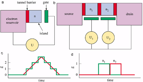
The basic building block of devices that can manipulate single charges is the “single-electron box” (see figure a). It consists of a small conducting electrode, known as an island, that is in contact with a charge-reservoir electrode via a thin insulating layer acting as tunnel barrier. The tunnel barrier is opaque enough to maintain charge quantization in the island, as if the island was surrounded by a perfect insulator. At the same time, however, the barrier is transparent enough to allow electrons to pass across it. A gate voltage U is applied between the reservoir and a gate electrode, which influences the island electrostatically.
This simple system is characterized by the number, n, of excess charge quanta on the island. (We assume that n is positive if there is an excess of electrons on the island and negative if there is a deficit.) The number of charge quanta is subject to two contradictory influences. On the one hand, n should adopt the value that minimizes the total electrostatic energy of the system. The characteristic energy involved is Ec = e2/2C, the energy of an excess electron with charge e on an island that has a total capacitance C when the gate voltage is zero.
On the other hand, the number of charge quanta is affected by thermal fluctuations that typically have energy kBT, where kB is the Boltzmann constant and T is the temperature. At sufficiently low temperatures (i.e. kBT Ec) the average value of n varies with the gate voltage in a stepwise fashion, each step corresponding to the arrival of one electron onto the island (see figure b). At higher temperatures, thermal fluctuations mask the charge quantization and the average value of n varies continuously.
The charge-transfer process in a single-electron box with one island is very easy to understand but is also too elementary for applications. Although we can add a well defined number of electrons to the island, the only thing that we can do next is to remove them, because the charge on the island cannot grow indefinitely. With two islands and two gate voltages, however, we can play a much more interesting game (see figure c). Using a suitable sequence of gate voltages, we can transfer a single electron from a source reservoir to the first island, then to the second and finally to a drain reservoir (figure d). This is the basis of the single-electron pump.
Ingenious fabrication
But it is not easy to implement islands that are linked to charge reservoirs through tunnel barriers in silicon. Ordinary silicon is a semiconductor, not a metal. A silicon wire can become conducting, however, in the presence of a large electric field (which can be applied via a gate electrode). The next problem is to interrupt this wire with tunnel barriers to create an isolated island that has a sufficiently small capacitance so that the energy of an excess electron exceeds the energy of any thermal fluctuations.
The NTT team uses a clever fabrication method. Fujiwara and Takahashi built their device from a silicon wire some 10-20 nm diameter. On top of this wire they deposit a metallic wire made of polysilicon, which crosses the silicon at right angles and is similar in width. A very thin insulating layer of silicon oxide separates the two wires. Such an arrangement produces an island for holes in the silicon wire. This island forms in the small overlap region under the metallic wire when the latter is raised to a large negative voltage.
The experiment, which involves transferring charge between two coupled islands, has another ingenious feature: the charge in each of the islands is detected with in situ metal-oxide-silicon transistors. The channels of the transistors are made of the same wire as the islands. Sensing electrons run on the “floor” of the wire, while single holes are stored on the “ceiling”. The electrons and holes are kept apart by a strong electric field that is perpendicular to the wire, and thus they do not recombine.
The experiment runs at 25 K, a temperature that is still very low compared with room temperature, but 50 times higher than the temperature needed to observe single-electron effects in conventional metallic systems. Cooling systems have been making steady progress to ever lower temperatures, and it is reasonable to assume that one day these chips could be cooled by a small portable refrigerator that runs on electricity, rather than liquid helium. However, to take full advantage of the single-electron transfer, computer architecture will probably have to change as well, and will perhaps be based on a new principle like the cellular automaton. No one seems to doubt that we will reach the ultimate limit of electronics one day. The question is when.