Microelectronic devices that exploit the spin of the electron as well as its charge promise to revolutionize the electronics industry. The challenge, as Tony Bland, Kiyoung Lee and Stephan Steinmüller describe, is to find a way of integrating semiconductors into such "spintronic" circuits
Eighty years ago theoretical physicists had a problem: they lacked a mathematical description of elementary particles that was consistent with the principles of both Einstein’s special theory of relativity and the newly formed theory of quantum mechanics. In 1927 Erwin Schrödinger had written down the quantum mechanical equation of motion for the electron, but this did not take into account the fact that electrons are relativistic particles. Troubled by this situation, Paul Dirac set about finding a solution.
The equation Dirac arrived at the following year was a mathematical tour de force, which predicted two totally unexpected physical phenomena. The first was the existence of antiparticles, which was proved in 1932 with the discovery of the positron (an anti-electron). The second was that the electron must have an intrinsic angular momentum or “spin” that has only two possible orientations in an applied magnetic field: aligned with the field, or “up”; and anti-aligned, or “down”.
The electron lies at the heart of the microelectronics revolution, where it is shuttled around in semiconductors (usually silicon) to allow transistors and other such devices to operate. Yet these devices — which underpin everything from microwave ovens to cosmological probes — only exploit the charge of the electron, while for 70 years following Dirac’s groundbreaking discovery the electron’s spin has largely been ignored by the device and semiconductor industry.
One reason for this is the phenomenal success in miniaturizing devices. For the last 40 years the number of transistors per unit area that can be etched onto a silicon chip — which, for example, governs the processing power of a computer — has doubled every 18 months, a trend known as Moore’s law. But we are now rapidly approaching the limit of how small and closely packed these transistors can become before the heat that they generate cannot be dissipated fast enough, or unwanted quantum-mechanical effects prevent them from functioning properly.
If Moore’s law is to continue, we need to find an alternative to conventional microelectronics — at long last it is time to exploit the electron’s spin in semiconductor devices. Whereas conventional electronic devices rely on only controlling the flow of charge, a “spintronic” device would also control the flow of electron spins (the so-called spin current) within the device, thereby adding an extra degree of freedom.
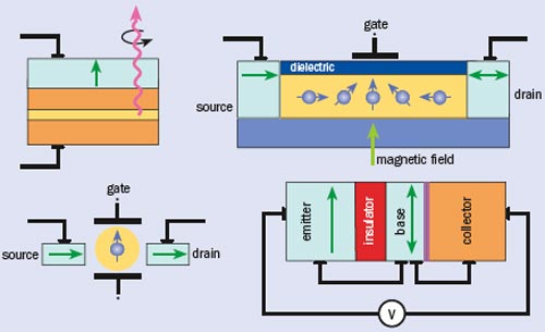
Because the spin of an electron can be switched from one state to another much faster than charge can be moved around a circuit, spintronic devices are expected to operate faster and produce less heat than conventional microelectronic components. One of the ultimate goals is to build a spin-based transistor that would replace conventional transistors in integrated logic circuits and memory devices, thus allowing the miniaturization trend to continue. However, spintronics also opens the door to entirely new types of device, such as a light-emitting diode (LED) that generates left or right circularly polarized light for use in encrypted communication (see “Spin-based devices”). Looking further into the future, spintronic devices could even be used as quantum bits, the units of information processed by quantum computers.
For the spintronics revolution to happen, however, researchers need to find a way to inject, manipulate and detect the spin of electrons in semiconductors, since these materials are likely to remain central to device physics for the foreseeable future. Spin manipulation should in theory be relatively straightforward, but injecting and detecting spin under practical conditions are huge challenges.
Giant achievement
Electron spin is already big business outside the semiconductor industry. In fact, metal-based spintronic devices can be found in the hard disks of virtually every computer on the planet. In 1988 Peter Grünberg at the Research Centre Jülich in Germany and Albert Fert at the Université Paris-Sud in France independently discovered that the flow of spin-polarized electrons between two thin layers of ferromagnetic metal separated by a layer of non-magnetic metal can be increased by about 3% by changing the relative magnetic alignment of the ferromagnetic layers from antiparallel to parallel — a discovery that earned them the 2007 Nobel Prize for Physics (see Physics World November 2007 p7, print edition only). This effect — called giant magnetoresistance (GMR) — made it possible for the magnetic read heads of hard disks to be much more sensitive to changes in magnetic fields, which boosts storage capacity by allowing information to be stored in much smaller regions on the disks’ surface.
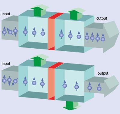
The ability to transport electron spins between two metals also underpins magnetoresistive random access memory (MRAM) — a novel type of computer memory that can retain information without requiring any power. MRAM is based on a similar effect to GMR known as tunnel magnetoresistance (TMR), which arises when two layers of ferromagnetic metal are separated by a thin layer of insulating material, such as aluminium oxide or magnesium oxide. Instead of the spin-polarized electrons diffusing slowly from one ferromagnetic layer to the other as happens in GMR, in TMR they tunnel quantum mechanically (a classically forbidden process in which a particle passes through a potential barrier higher than its kinetic energy) through the barrier layer — as such these devices are called magnetic tunnel junctions (MTJs) (see “Magnetic tunnel junction”). The Pauli exclusion principle then comes into play. Tunnelling — and therefore spin transport across the barrier — can only occur if empty (i.e. unoccupied) wave states with the same spin are available on the other side of the barrier: the result is spin-dependent tunnelling.
Such spin-dependent tunnelling was demonstrated at low temperatures in 1975 by Michel Jullière at the Institut National des Sciences Appliquées de Lyon in France. But it was not until 1995 that Terunobu Miyazaki at Tohoku University in Japan and Jagadeesh Moodera at the Massachusetts Institute of Technology (MIT) in the US independently showed that it was possible to achieve TMR at room temperature. Unfortunately, the change in tunnel current as the spin alignment of the ferromagnetic layers is switched between parallel and antiparallel — known as the TMR ratio — was just 12–18% in Miyazaki’s and Moodera’s devices, which is far below what was needed to make a practical memory device. However, thanks to a major research programme on tunnel magnetoresistance supported by the Defense Advanced Research Projects Agency (DARPA) in the US, as well as a significant industrial research effort, the TMR ratio was eventually increased to 70% by the late 1990s.
More recently, the ability to fabricate atomically flat interfaces between the metal and the oxide layers has enabled Stuart Parkin’s group at IBM’s Almaden Research Center in California, and Shinji Yuasa and colleagues at the AIST in Japan to independently achieve TMR values of about 400% via coherent tunnelling. TMR-based commercial MRAM arrays are already starting to become available, and these could one day be used to build PCs that switch on instantly.
TMR relies on a large number of electrons with the desired spin state being transmitted across interfaces between ferromagnetic metals and insulating metal oxides. To make semiconductor spintronic devices possible, however, we need to achieve such behaviour across interfaces formed between a semiconductor and a material that can serve as a spin injector or detector.
Magnetic appeal
Silicon and gallium arsenide are the two most widely used semiconductors, so the challenge is to find spinpolarized materials — i.e. materials in which most of the electron spins are aligned in a particular direction — that can be combined with them. Promising candidates are “dilute magnetic semiconductors” (DMS) — semiconductors that, when doped with impurity atoms, display ferromagnetism.
In 1999 two groups independently injected spinpolarized electrons from a magnetic semiconductor into gallium arsenide. Laurens Molenkamp and colleagues at Würzburg University, Germany, maintained a polarization of 90% during spin injection from a spinpolarized semiconductor material into a gallium-arsenide structure at low temperature, although the semiconductor injector required an external magnetic field to maintain its polarization. Hideo Ohno’s group in Tohoku, Japan, in collaboration with David Awschalom’s group at the University of California, Santa Barbara, on the other hand, managed the same feat from a “true” DMS that does not require an applied magnetic field, although the researchers only achieved an injected spin polarization of about 1%. Together, these experiments demonstrated that it was possible to inject spin into a semiconductor; to develop a practical device, the next step was to find DMS materials that would allow robust spin injection at room temperature with only modest (or zero) applied fields.
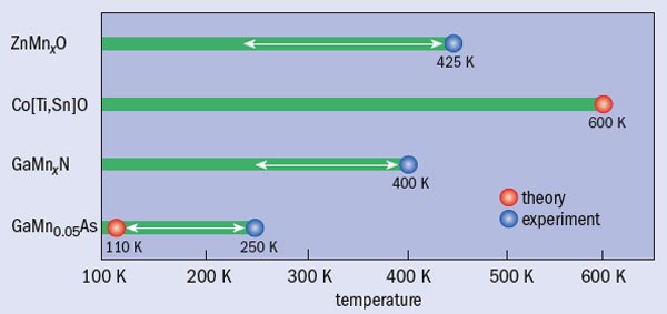
In 2000 Thomas Dietl of the Polish Academy of Sciences in Warsaw made an important breakthrough in this regard. He showed that the highest (Curie) temperature at which ferromagnetism occurs in certain DMS materials should increase significantly as they are doped with increasing concentrations of, in particular, the magnetic elements manganese or cobalt. His calculations were based on a concept first proposed by the late US physicist Clarence Zener in the 1950s, in which interactions between the magnetic moments of the localized impurity atoms and those of the delocalized holes in the semiconductor can cause the moments to align as they would in a ferromagnet. Furthermore, this effect should overcome the misaligning effect that is caused by high temperatures. Notably, Dietl’s calculations suggested that the commonly used semiconductors zinc oxide and gallium nitride should, with sufficient doping, exhibit ferromagnetism well above room temperature, thus sparking a major worldwide effort to develop practical DMS materials (see “Raising the Curie temperature”).
Finding a material that exhibits spin polarization well above room temperature, however, is not the only challenge in developing a practical spin injector. First, it must have a large polarization in order to be able to inject enough spin-polarized electrons into a semiconductor. Second, it must be possible to control the properties of the interface that forms when the injector material is deposited on the semiconductor. While developing magnetic tunnel junctions in the 1990s, researchers learned that the properties of the few atomic layers close to the interface have a critical effect on spin-injection efficiency. This is because very small amounts of chemical intermixing between the layers can scatter the electrons into new states and therefore substantially lower the amount of electrons that make it across the interface while remaining polarized. It is difficult to control the properties of DMS materials in bulk form, and even more so when the material is deposited in a thin film, as is required when fabricating a device. Achieving clean interfaces between DMS materials and semiconductors, therefore, poses a considerable challenge for researchers trying to build DMS-based spintronic devices.
Tunnel vision
There is, however, an alternative and fundamentally different approach to achieving spin injection. While many researchers concentrated on DMS materials, others reasoned that if spin-polarized electrons could be transmitted across an interface between a semiconductor and a ferromagnetic metal, the metal could then be used as a highly effective spin polarizer. Furthermore, since metal interfaces have been studied for decades, it should be much easier to control the interface properties in such device structures.
In the late 1990s several research groups attempted to inject spin-polarized electrons from ferromagnetic metals and alloys deposited directly onto gallium arsenide, but these early studies achieved injected polarizations of just a few per cent. A further blow to the idea was dealt in 2000, when Georg Schmidt and colleagues at Würzburg University used a simple model of a resistor network to show that a spin polarization of nearly 100% would be needed in the ferromagnetic metal in order to inject a useful spin polarization into the semiconductor. Such high polarizations are impossible to achieve in practice, so for a brief period it seemed that semiconductor spin injectors were likely to be the only possible way forward.
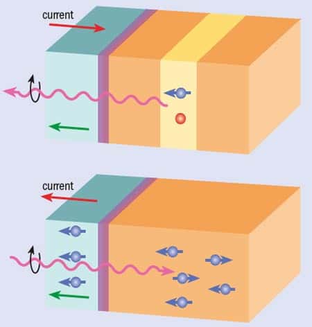
This view was turned on its head almost immediately, however, when Emmanuel Rashba at MIT realized that creating a tunnel barrier between the ferromagnetic metal and the semiconductor would solve the problem. He predicted that the spin polarization in the conductive metal would be preserved during tunnelling, and therefore that the ferromagnetic-metal–barrier spin injector was analogous to a magnetic tunnel junction. Following this development, a concerted effort was made to investigate the injected spin polarization in a ferromagnetic-metal–gallium-arsenide structure. In such samples, electrical charge is redistributed as the junction between the metal and the semiconductor forms, thus creating a “Schottky” tunnel barrier at the interface. It turns out that this type of structure also demonstrates the concept of a spin-LED (see “Electro-optical injection and detection”): when a polarized electron is injected from the ferromagnetic layer into the semiconductor, it recombines with a hole, which results in the emission of circularly polarized light. (In a conventional LED, in contrast, unpolarized electrons and holes combine to produce unpolarized light.) Several research groups are currently trying to exploit this phenomenon to develop a practical spin-LED device.
Since the number of spin-polarized electrons that make it across the barrier depends on its properties, however, some researchers tried replacing the Schottky barrier with a thin insulating layer in an attempt to increase the spin-injection signal in ferromagnetic-metal–semiconductor systems. In 2003 Pol Van Dorpe and colleagues at the Interuniversity Microelectronics Centre (IMEC) in Leuven, Belgium, achieved an injected spin polarization of just over 20% at low temperature with an aluminium-oxide insulating layer. Then, two years later, Parkin’s group at IBM showed that using magnesium oxide as an insulator improved the performance further, but that the injected polarization is highly sensitive to the crystal structure of the barrier material.
Meanwhile, progress was also being made in the other big challenge that needs to be overcome in order to build a spintronic device: spin detection. One way to do this is to reverse the process that allows a spin-LED to work (see “Electro-optical injection and detection”). By shining polarized light at a ferromagnetic-metal–Schottky-barrier–gallium-arsenide heterostructure, a population of spin-polarized electrons is generated within the gallium-arsenide substrate (via the optical-selection rules for this semiconductor). These electrons can then tunnel back across the Schottky barrier into the ferromagnetic metal where they can be detected electrically, so offering a way to detect electron spins. In 2004 our group in Cambridge used such a structure to show that this effect produces a voltage that depends on the percentage of the electrons in the ferromagnetic metal that are polarized.
Since then, we have found that by replacing the single layer of ferromagnetic metal with a metal GMR spin valve (i.e. two thin layers of ferromagnetic metal separated by a thin layer of non-magnetic metal), the current flowing into the metal can be determined separately from the current flowing in the semiconductor, since the valve acts as a gate that switches the current flowing to the metal on or off according to the magnetic alignment of its layers. Using the spin valve in this way allowed us to quantify the spin-filtering effect of the interface; and hence estimate the polarization of the detected current.
Interface matters
We are now six years on from Dietl’s predictions that the Curie temperature of certain DMS materials should increase significantly with ferromagnetic doping. Yet still no-one has found suitable ferromagnetic semiconductor materials that operate at room temperature and can be used in practical semiconductor spintronic devices. While the effort to develop DMS-based spintronics continues, however, the remarkable development of magnetic tunnel junction technology has given great impetus to using ferromagnetic metals in combination with semiconductors. While ferromagnetic transition metals do not offer 100% spin polarization, this may not be necessary for practical devices: theoretical predictions suggest that by controlling the interface structure and composition, and using appropriate barriers, future ferromagnetic-metal systems could yield dramatic increases in spin transmission over the injector/detector materials tried so far.
The successful development of MTJs has already shown that the properties of the few atomic layers close to the interface have a critical effect on spin transmission. In the future it will be important to precisely control the structure of the materials used in semiconductor spintronic devices by matching the crystal orientation of the interface with that of the spin injector/detector material, and it is clear that there are many promising new routes to investigate. While it is not possible to say how long this will take, it looks increasingly likely that the semiconductor spintronics revolution will be kicked off by devices that use the magnetic transition metal films already found in MRAM and MTJ devices.
At a Glance: Semiconductor spintronics
- In addition to their charge, electrons have an intrinsic angular momentum or “spin” that has only two possible orientations in an external magnetic field
- The electron spin is currently exploited in computer hard disks and magnetoresistive random access memory via the giant magnetoresistance and tunnel magnetoresistance effects, which occur in layered metal structures
- Semiconductor devices that exploit spin as well as charge would operate faster than conventional microelectronic devices and would offer new functionality
- The main challenge in building such a device is transporting spin-polarized electrons efficiently into and out of the semiconductor region of the device
- Currently, researchers are following two approaches to spin injection and detection: dilute magnetic semiconductors deposited onto conventional semiconductors; and ferromagnetic metals deposited onto semiconductors
More about: Semiconductor spintronics
D D Awschalom et al. 2007 The diamond age of spintronics Scientific American 297 58
J A C Bland et al. 2005 Optical studies of electron spin transmission Ultrathin Magnetic Structures IV (ed) B Heinrich and J A C Bland (Springer, New York) pp59–100
T Dietl 2003 Dilute magnetic semiconductor: functional ferromagnets Nature Materials 2 646
B T Jonker and M E Flatté 2006 Electrical spin injection and transport in semiconductors Nanomagnetism (ed) D L Mills and J A C Bland (Elsevier, Amsterdam) pp227–272
H Ohno et al. 2000 Electric-field control of ferromagnetism Nature 408 944
S A Wolf et al. 2001 Spintronics: A spin-based electronics vision for the future Science 294 1488
I Zutic et al. 2004 Spintronics: fundamentals and applications Rev. Mod. Phys. 76 323
• Physics World notes with regret the death of Professor Tony Bland shortly after the completion of this article. An obituary appears on page 9 (print edition only).
