Photons in arrays of nanometre-sized structures exhibit more complex behaviour than electrons in conventional solid-state materials. Though the two systems are sometimes treated as analogous, scientists at the University of Twente in the Netherlands discovered variations in the shape of the photons’ orbitals. These variations, they say, could be exploited when designing advanced optical devices for quantum circuits and nanosensors.
In solid-state materials, electrons are largely confined to regions of space around atomic nuclei known as orbitals. Additional electrons stack up in these orbitals in bands of increasing energy, and the scientists expected to find similar behaviour in photons. “It has been known for some time that photonic materials are similar to standard electronic matter in many ways and can be described using energy bands and orbitals, too,” says Marek Kozon, a theorist and mathematician who participated in the study as part of his PhD in the Complex Photonic Systems (COPS) lab at Twente.
“Similar” does not mean “same”, however. “We have now discovered that orbitals in which photons are confined are significantly more varied in shape than electronic orbitals,” Kozon says. This is important, he says, because the shape of electronic orbitals influences materials’ chemical properties – something that is apparent in the Periodic Table of the Elements, which groups elements with similar orbital structures together. Additional variations in the shape of photonic orbitals could also create properties not achievable in electronic materials.
Boring electrons, exciting photons
The comparatively “boring” behaviour of electrons stems from the fact that they always orbit the nucleus in regions with sphere-like shapes, explains Kozon, who is now at the single-photon detector company Pixel Photonics in Germany. Photonic materials, in contrast, can be designed with much more freedom.
In the latest work, the Twente researchers used numerical computations to study how photons behave when they are confined in a three-dimensional nanostructure known as an inverse woodpile superlattice. This superlattice is a photonic crystal that contains periodic defects with a radius that differs from that of the pores in the underlying structure. The researchers adopted this design for two reasons, Kozon explains. The first is that photonic states inside the defects are insulated from their environment, making them easier to study. The second is that 3D inverse woodpile superlattices are relevant to experiments being carried out by colleagues in the COPS lab.
The team’s original motivation, Kozon continues, was to better understand how light is confined in these structures. “The study turned out be significantly more complicated than we expected,” he says. “We produced several terabytes of data and developed new analysis methods, including scaling and machine learning, to evaluate the sheer amount the information we had gathered. We then investigated in more detail the superlattice parameters that the analysis flagged up as the most interesting.”
Applying the scaling techniques, for example, created an unexpected issue. While scaling theories usually work well for very large systems, which in this case would mean very large periodicities (or lattice constant), Kozon notes that “our system is precisely the opposite because it has a small periodicity. We were thus not able to calculate how light behaves in it.”
Optimally confining light
The team solved this problem by developing a unique clustering method that uses unsupervised machine learning to analyse the data. Thanks to these analyses, the researchers now know which types of structures can optimally confine light in an inverse woodpile superlattice. Conversely, they can identify any deviations from these ideal structures by comparing experimental observations with their – now vast – database.
Direct image of an electron orbit in an exciton is a first, say researchers
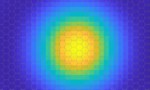
And that is not all: the team also analysed where energy is concentrated in the photonic crystal, making it possible to determine which parameters allow the greatest concentration of energy in a small volume of the structure. “This is extremely important for so-called cavity-quantum-electrodynamics (QED) applications in which we force light to interact with matter and, for example, to control the emission of light sources or even create exotic states of mixed light and matter,” Kozon tells Physics World. “This finding could help advance applications in efficient lighting, quantum computing or sensitive photonic sensors.”
The Twente researchers are now fabricating real 3D superlattices thanks to the knowledge they have gained. They report their present work in Physical Review B.