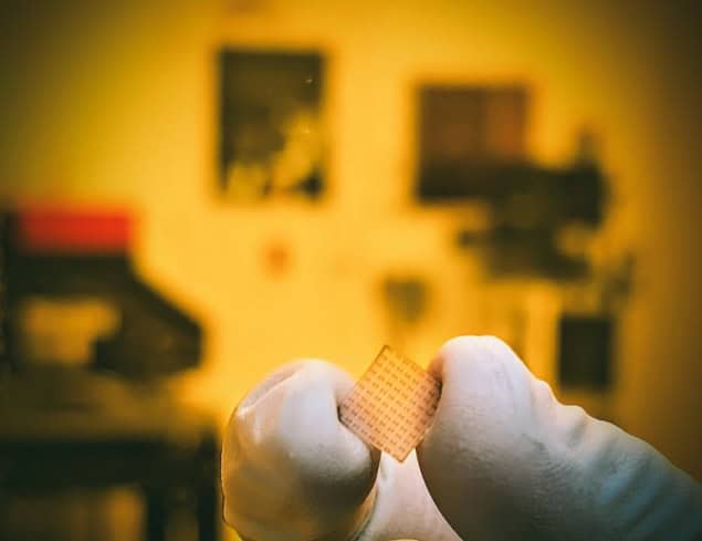
Metals usually become less conductive as they get thinner. Niobium phosphide, however, is different. According to researchers at Stanford University, US, a very thin film of this non-crystalline topological semimetal conducts electricity better than copper even in non-crystalline films. This surprising result could aid the development of ultrathin low-resistivity wires for nanoelectronics applications.
“As today’s electronic devices and chips become smaller and more complex, the ultrathin metallic wires that carry electrical signals within these chips can become a bottleneck when they are scaled down,” explains study leader Asir Intisar Khan, a visiting postdoctoral scholar and former PhD student in Eric Pop’s group at Stanford.
The solution, he says, is to create ultrathin conductors with a lower electrical resistivity to make the metal interconnects that enable dense logic and memory operations within neuromorphic and spintronic devices. “Low resistance will lead to lower voltage drops and lower signal delays, ultimately helping to reduce power dissipation at the system level,” Khan says.
The problem is that the resistivity of conventional metals increases when they are made into thin films. The thinner the film, the less good it is at conducting electricity.
Topological semimetals are different
Topological semimetals are different. Analogous to the better-known topological insulators, which conduct electricity along special edge states while remaining insulating in their bulk, these materials can carry large amounts of current along their surface even when their structure is somewhat disordered. Crucially, they maintain this surface-conducting property even as they are thinned down.
In the new work, Khan and colleagues found that the effective resistivity of non-crystalline films of niobium phosphide (NbP) decreases dramatically as the film thickness is reduced. Indeed, the thinnest films (< 5 nm) have resistivities lower than conventional metals like copper of similar thicknesses at room temperature.
Another advantage is that these films can be created and deposited on substrates at relatively low temperatures (around 400 °C). This makes them compatible with modern semiconductor and chip fabrication processes such as industrial back-end-of-line (BEOL). Such materials would therefore be relatively easy to integrate into state-of-the-art nanoelectronics. The fact that the films are non-crystalline is also an important practical advantage.
A “huge” collaboration
Khan says he began thinking about this project in 2022 after discussions with a colleague, Ching-Tzu Chen, from IBM’s TJ Watson Research Center. “At IBM, they were exploring the theory concept of using topological semimetals for this purpose,” he recalls. “Upon further discussion with Prof. Eric Pop, we wanted to explore the possibility of experimental realization of thin films of such semimetals at Stanford.”
Surface superconductivity appears in topological materials
This turned out to more difficult than expected, he says. While physicists have been experimenting with single crystals of bulk NbP and this class of topological semimetals since 2015, fabricating them at the ultrathin film limit of less than 5 nm at a temperature and using deposition methods compatible with industry and nanoelectronic fabrication was new. “We therefore had to optimize the deposition process from a variety of angles: substrate choice, strain engineering, temperature, pressure and stoichiometry, to name a few,” Khan tells Physics World.
The project turned out to be a “huge” collaboration in the end, with researchers from Stanford, Ajou University, Korea, and IBM Watson all getting involved, he adds.
The researchers says they will now be running further tests on their material. “We also think NbP is not the only material with this property, so there’s much more to discover,” Pop says.
The results are detailed in Science.


