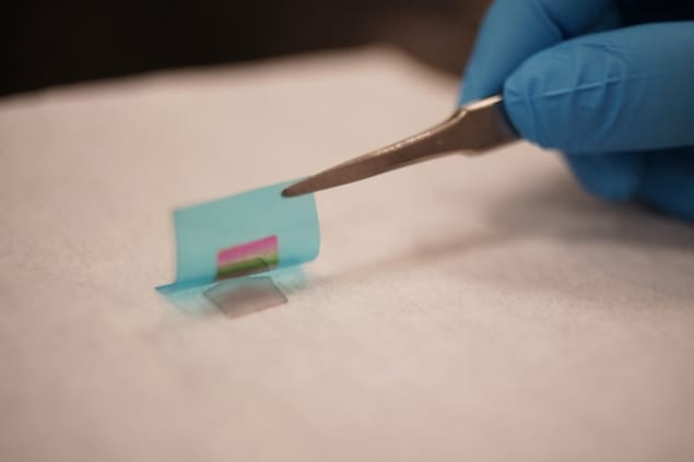
A new “remote epitaxy” technique developed by researchers at the Massachusetts Institute of Technology (MIT) that exploits the “transparency” of graphene to atomic interactions could be used to fabricate ultrathin flexible films of a variety of semiconducting materials on non-silicon wafers. These films could be used to make functional components for use in a host of electronics devices, including wearable sensors and flexible solar cells.
Modern electronics is largely based on silicon, which is the most abundant – although certainly not the best – semiconducting material on Earth. Although other substrates, such as gallium arsenide (GaAs) and gallium nitride (GaN) are much better, they are a lot more expensive.
Although a routinely employed technique to fabricate electronics devices, epitaxial growth is far from straightforward. Growing different crystalline materials on top of each other is no easy task since their lattice parameters need to be carefully matched as do the surface energies across the interfaces between the epilayer and the bulk substrate. Another difficulty is that the films cannot be easily removed from the growth substrate, so this wafer cannot be reused.
Two teams of researchers led by Jeffrey Grossman and Jeehwan Kim are now saying that they have developed a new way to grow ultrathin and flexible films of a variety of semiconductors on substrates other than silicon – that can then be reused.
The invisibility of graphene
Last year, Kim and colleagues discovered that stacking graphene on top of a GaAs wafer and then flowing atoms of Ga and As over the stack resulted in the atoms assembling into a pattern that “copied” that of the single-crystalline pattern of the underlying GaAs wafer. It was as if the graphene was transparent, or invisible, they say. What is more, they found that they could easily peel the resulting epitaxially-grown film away from the graphene layer, leaving the GaAs wafer untouched and ready to be used again.
Repeating their experiments with wafers made from other semiconducting materials, such as silicon (Si) and germanium (Ge) did not produce the same results, however. Flowing atoms of Si and Ge did not interact with the underlying wafers and the graphene acted as a “barrier” between the wafer and the atoms in this case.
Self-assembled molecular layers strike a balance
Polarity matters
“This is because the polarity of the 2D materials plays a crucial role in determining the transparency of these materials to remote atomic interactions,” explains Kim. Indeed, the atoms can only interact with each other and “ignore” the intermediate graphene layer if they have different ionic charges. This is not the case for Si and Ge, which have the same ionic charge because they both belong to the same group (IV) of the periodic table. They thus do not interact with each other. Ga and As, on the other hand, are positively and negatively charged, respectively, and thus do.
“The greater the degree of polarity, the stronger the atomic interaction,” says Kim.
The polarity of the substrate itself also matters, he adds. Hexagonal boron nitride (hBN), for example, which is similar in crystalline structure to graphene, contains oppositely charged boron and nitrogen atoms. Any atoms flowing over this substrate, even if they are highly polarized themselves, cannot interact with the underlying hBN wafer.
The new technique, which is detailed in Nature Materials 10.1038/s41563-018-0176-4, could thus be used fabricate ultrathin flexible thin films from a variety of semiconducting compounds as long as they contain oppositely charged atoms, he explains. These films could be stacked on top of each other to produce functional devices, such as wearable sensors and flexible solar cells. “Indeed, we will now be looking at stacking freestanding single crystalline semiconductors made using our remote epitaxy technique to make unique heterostructures for IoT applications or medical devices,” he tells Physics World.


