A light-emitting silicon-based material with a direct band gap has been created in the lab, 50 years after its electronic properties were first predicted. This feat was achieved by an international team led by Erik Bakkers at Eindhoven University of Technology in the Netherlands. They describe the new nanowire material as the “Holy Grail” of microelectronics. With further work, light-emitting silicon-based devices could be used to create low-cost components for optical communications, computing, solar energy and spectroscopy.
Silicon is the wonder material of electronics. It is cheap and plentiful and can be fabricated into ever smaller transistors that can be packed onto chips at increasing densities. But silicon has a fatal flaw when it comes to being used as a light source or solar cell. The semiconductor has an “indirect” electronic band gap, which means that electronic transitions between the material’s valence and conduction bands involve vibrations in the crystal lattice. As a result, it is very unlikely that an excited electron in the conduction band of silicon will decay to the valence band by emitting light. Conversely, the absorption of light by silicon does not tend to excite valence electrons into the conduction band – a requirement of a solar cell.
In contrast, electronic transitions in direct band gap semiconductors do not involve lattice vibrations, so these materials emit copious amounts of light when electrons are excited – and are very good at converting light into electricity.
Incompatible with silicon processing
As a result, direct band gap materials such as gallium arsenide are used to create LEDs, lasers and solar cells. Unfortunately, these materials are hard to integrate into silicon processing, making it difficult and expensive to create devices that combine the electronic properties and scalability of silicon with the optical properties of direct band gap materials. Such devices could, in principle, lead to faster and more efficient telecoms and computing systems in which information is transmitted and processed using light alone.
50 years ago, researchers first calculated that a silicon-germanium alloy with a hexagonal crystal structure should have a direct band gap. The problem is that under ambient conditions both silicon and germanium have diamond-like crystal structures.
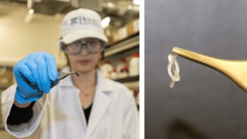
In 2015 Bakkers’ team developed a way of creating hexagonal germanium and silicon germanium nanowires. This involves first growing an extremely thin (about 35 nm diameter) gallium arsenide nanowire substrate. Germanium is then deposited on the nanowire, increasing its thickness by a factor of 10. The gallium arsenide nanowires have a hexagonal cross section and as a result, the surrounding germanium shell also has a hexagonal crystal structure. This is because the gallium arsenide provides a structural template for hexagonal growth; and the very high surface to volume ratio of the nanowire allows hexagonal growth to occur.
Once they created the hexagonal germanium shell, the researchers were able to deposit silicon-germanium or silicon to create hexagonal crystals of those materials. “We were able to do this such that the silicon atoms are built on the hexagonal template, and by this forced the silicon atoms to grow in the hexagonal structure,” explains Eindhoven’s Elham Fadaly.
Defects and impurities
In 2015, however, they were unable to make the nanowires emit light – a problem that the team said was related to the presence of defects and impurities in the crystal structure.
Now, the Eindhoven team has joined forces with researchers in Germany and Austria to create higher quality nanowires that emit light. They measured the emission by firing a laser at the nanowires in order to excite the electrons and then detected the infrared light that is emitted. “Our experiments showed that the material has the right structure, and that it is free of defects. It emits light very efficiently,” says Eindhoven’s Alain Dijkstra.
First light for germanium laser
The researchers found that by reducing the silicon content of the hexagonal alloy from 35% to 0 they could change the wavelength of the light from 1.5 to 3.5 µm. This partially overlaps the wavelengths of infrared light that are currently used in optical telecoms.
Bakkers believes that the team will soon be able to create a laser using the nanowires: “By now we have realized optical properties that are almost comparable to indium phosphide and gallium arsenide, and the materials quality is steeply improving. If things run smoothly, we can create a silicon-based laser in 2020.”
As well as optical telecoms and optical computing, the new silicon-based material could be used to create low-cost chemical sensors that use infrared spectroscopy.
The research is described in Nature.


