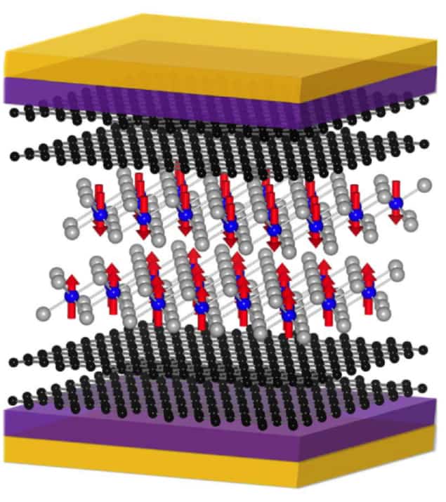
Transistors that make use of the spin magnetic moment of an electron rather than its charge could be used to make devices that are smaller and more energy efficient than conventional electronics. Individual electron spins – which can point up or down – could also be used to store and transfer information in computers. Such devices are challenging to make, however. Researchers at Cornell University in the US have now succeeded in fabricating a new spin tunnel field-effect transistor (TFET) from a 2D van der Waals material that can be switched between high and low resistance states using an applied electric field. The device could help in the development of real-world, high-performance spin-FETs in the future.
Spin-FETs are electrically switching devices that can be turned on and off by controlling electron spin rather than electronic charge and they were first proposed by Supriyo Datta and Biswajit Das in 1990. Compared to conventional transistors that operate by controlling charge current, which causes significant Joule heating, spin-FETs are much more energy-efficient because they do not suffer from this problem.
Making spin-FETs based on Datta and Das’ idea is no easy task, however, because they require precise electric-field control of spin current in a semiconductor channel, explains Kin Fai Mak, who led this research effort. Spin injection is an inefficient process and the fact that electron spins do not travel very far in most materials means that information being carried by these spins is also quickly lost. The main problem here is spin relaxation: as electrons travel through a material, the direction of the electron’s spin is randomized by scattering events.
Completely different principle
“Instead of realizing Datta and Das’ original idea, we built a spin-TFET based on a completely different principle that does not require electric field control of spin current, says Mak. “We instead operate our device by flipping the spins in the TFETs’ magnetic tunnel barrier using electric fields.”
Such spin flipping significantly modulates the device resistance, which leads to a spin-FET that requires no spin current injection and therefore does not suffer from spin relaxation. “Although our spin-FET is yet far from any real-world applications (it only works at cryogenic temperatures for one), the idea could inspire new way of realizing practical and high-performance spin-FETs in the future.”
Mak and colleagues made their device by mechanically exfoliating 2D layers of the magnetic insulator chromium triiodide (CrI3) using the now famous “sticky tape” method, which was first used to isolate graphene. The researchers placed layers of graphene, CrI3 and graphene again onto a substrate and then built the spin-TFET by transferring the different material layers on top of each other.
Scaling up
“Our device consists of a graphene/CrI3/graphene vertical junction with top and bottom gates,” explains Mak. “The two nearly symmetric gates are made of few-layer graphite gate electrodes and hexagonal boron nitride (hBN) gate dielectrics that are around 30 nm thick.”
Although the technique is quite low-tech at this point, we expect that people will be able to use epitaxial growth techniques in the future, which will allow for a much more scalable device architecture, he says.
The researchers say they are nonetheless able to build tunnel junction devices with high quality interfaces and the desired magnetic and electrical properties using their basic technique.
“We are able to achieve an on-off ratio of up to 400% in our spin-TFET by electrically flipping spins in the CrI3 magnetic tunnel barrier layer,” Mak tells Physics World. “Spin flipping leads to a high-low resistance state thanks to an effect known as spin filtering in which electrons with spins parallel to the spin filter (the CrI3) have a higher probability of being transmitted than those with spins perpendicular to the filter.
“Since the transmission probability is exponentially suppressed by quantum mechanical tunnelling, we observe a high on-off ratio, which could be improved further.”
Towards zero applied magnetic field
As well as finding use in energy-efficient computing and data storage, another potential application for the spin-TFETs is in electric-field-controlled MRAM devices, adds Mak. Compared to current MRAM technology that operates thanks to charge current control, electric field control consumes much less power and is therefore very efficient.
The researchers, reporting their work in Nature Electronics, say they are now busy improving their devices. “First, we would like to be able to make them work under zero applied magnetic field,” explains Mak. “The spin-FET we have demonstrated still requires an external magnetic field, which is not desirable for real technology applications.
Faster spin flipping and room temperature operation
“Second, we want to test the speed of the spin flipping process. Real devices require spin flipping rates in the gigahertz regime or higher so we must test the speed limit in our transistors and develop new ways to make it switch faster.”
Finally, the transistors need to operate at room temperature, which is not the case for the present devices. “Our spin-TFET is only a proof of concept but we hope our idea will stimulate the search for suitable materials systems that can used to make room-temperature devices in the future.”


