Electronics made from certain atomically thin materials can survive harsh radiation environments up to 100 times longer than traditional silicon-based devices. This finding, which comes from researchers at Fudan University in Shanghai, China, could bring significant benefits for satellites and other spacecraft, which are prone to damage from intense cosmic radiation.
Cosmic radiation consists of a mixture of heavy ions and cosmic rays, which are high-energy protons, electrons and atomic nuclei. The Earth’s magnetic field protects us from 99.9% of this ionizing radiation, and our atmosphere significantly attenuates the rest. Space-based electronics, however, have no such protection, and this radiation can damage or even destroy them.
Adding radiation shielding to spacecraft mitigates these harmful effects, but the extra weight and power consumption increases the spacecraft’s costs. “This conflicts with the requirements of future spacecraft, which call for lightweight and cost-effective architectures,” says team leader Peng Zhou, a physicist in Fudan’s College of Integrated Circuits and Micro-Nano Electronics. “Implementing radiation tolerant electronic circuits is therefore an important challenge and if we can find materials that are intrinsically robust to this radiation, we could incorporate these directly into the design of onboard electronic circuits.”
Promising transition-metal dichalcogenides
Previous research had suggested that 2D materials might fit the bill, with transistors based on transition-metal dichalcogenides appearing particularly promising. Within this family of materials, 2D molybdenum disulphide (MoS2) proved especially robust to irradiation-induced defects, and Zhou points out that its electrical, mechanical and thermal properties are also highly attractive for space applications.
The studies that revealed these advantages were, however, largely limited to simulations and ground-based experiments. This meant they were unable to fully replicate the complex and dynamic radiation fields such circuits would encounter under real space conditions.
Better than NMOS transistors
In their work, Zhou and colleagues set out to fill this gap. After growing monolayer 2D MoS2 using chemical vapour deposition, they used this material to fabricate field-effect transistors. They then exposed these transistors to 10 Mrad of gamma-ray irradiation and looked for changes to their structure using several techniques, including cross-sectional transmission electron microscopy (TEM) imaging and corresponding energy-dispersive spectroscopy (EDS) mapping.
These measurements indicated that the 2D MoS2 in the transistors was about 0.7 nm thick (typical for a monolayer structure) and showed no obvious signs of defects or damage. Subsequent Raman characterization on five sites within the MoS2 film confirmed the devices’ structural integrity.
The researchers then turned their attention to the transistors’ electrical properties. They found that even after irradiation, the transistors’ on-off ratios remained ultra-high, at about 108. They note that this is considerably better than a similarly-sized Si N-channel metal–oxide–semiconductor (NMOS) transistors fabricated through a CMOS process, for which the on-off ratio decreased by a factor of more than 4000 after the same 10 Mrad irradiation.
The team also found that MoS2 system consumes only about 49.9 mW per channel, making its power requirement at least five times lower than the NMOS one. This is important owing to the strict energy limitations and stringent power budgets of spacecraft, Zhou says.
Surviving the space environment
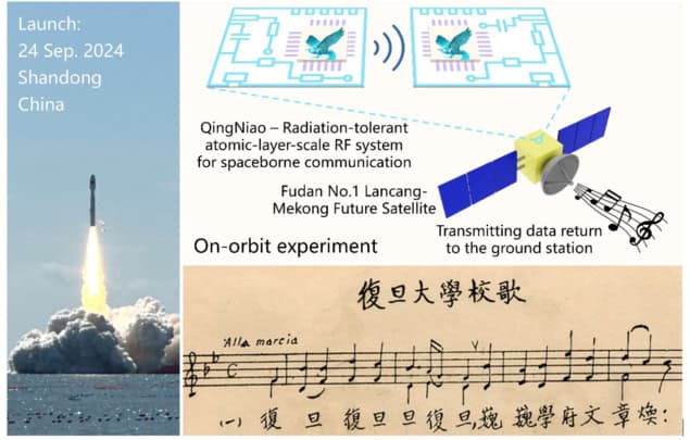
In their final experiment, the researchers tested their MoS2 structures on a spacecraft orbiting at an altitude of 517 km, similar to the low-Earth orbit of many communication satellites. These tests showed that the bit-error rate in data transmitted from the structures remained below 10-8 even after nine months of operation, which Zhou says indicates significant radiation and long-term stability. Indeed, based on test data, electronic devices made from these 2D materials could operate for 271 years in geosynchronous orbit – 100 times longer than conventional silicon electronics.
Thinner solar cells are more robust to space radiation
“The discovery of intrinsic radiation tolerance in atomically thin 2D materials, and the successful on-orbit validation of the atomic-layer semiconductor-based spaceborne radio-frequency communication system have opened a uniquely promising pathway for space electronics leveraging 2D materials,” Zhou says. “And their exceptionally long operational lifetimes and ultra-low power consumption establishes the unique competitiveness of 2D electronic systems in frontier space missions, such as deep-space exploration, high-Earth-orbit satellites and even interplanetary communications.”
The researchers are now working to optimize these structures by employing advanced fabrication processes and circuit designs. Their goal is to improve certain key performance parameters of spaceborne radio-frequency chips employed in inter-satellite and satellite-to-ground communications. “We also plan to develop an atomic-layer semiconductor-based radiation-tolerant computing platform, providing core technological support for future orbital data centres, highly autonomous satellites and deep-space probes,” Zhou tells Physics World.
The researchers describe their work in Nature.


