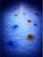
Researchers at Caltech are the first to image the distinct stages of a eutectic transformation, where a liquid transforms into two solid phases upon cooling. They achieved this by using 4D electron microscopy, which has high resolution in both space and time dimensions, at the nanometre and nanosecond level. The ability to probe and control eutectic reactions at the nanoscale can enable profound industrial advances, such as designing nanostructural alloys and solders.
Atoms move at ultrahigh speeds in eutectic reactions, which can take as little as 100 nanoseconds to complete. Hence 4D electron microscopy with high resolution in both 3D space and time is needed to capture the eutectic reactions in nanostructures as they progress.
The Caltech scientists initiated the eutectic reaction with a laser heating pulse. They then followed this with photo-generated single electron pulses, which can capture the state of the nanostructure at certain times after the initiation. The single electron pulse images can reveal when the solid phases nucleate, grow and solidify during the eutectic transformation with nanosecond accuracy.
Au-Ga-As system
Lead author Bin Chen and his team chose to study GaAs nanowires each capped with a gold nanoparticle. There have been many studies on eutectic reactions involving two elements, but not for three or more elements. Hence investigating the Au-Ga-As system can provide insights for more complex material systems.
With repeated laser excitations, the GaAs nanowires shrunk in length while the gold nanoparticle caps grew larger. The researchers can distinguish between the two eutectic solids formed – AuGa and AuGa2 – using diffraction patterns in normal transmission electron microscopy mode. They could directly control the eutectic transformation process and the resulting nanostructure by varying the intensity, polarization and number of laser heating pulses.
Set up of 4D electron microscope experiment
To achieve the above results, the researchers had to set up the experiment in a clever way. They designed the growth of the GaAs nanowires such that the nanowires stand with their long axis perpendicular to the substrate. In the transmission electron microscope, the substrate was rotated until it was parallel to the electron beam. By growing the nanowires several microns apart, they were spaced out enough to make any overlap in their profiles unlikely, but close enough to each other for the researchers to study several nanowires at once in statistical investigations. In addition, the non-destructive sample preparation of the as-grown nanowires allows for both qualitative and quantitative studies of the anisotropic nanowire properties in their native environment, free from environmental disturbances.
Having captured eutectic reactions successfully, 4D microscopy has far-reaching applications in other complicated material systems, in fields from photochemistry to biology. More directly related to the results of this study, the laser heating pulses can be used to accurately control the bonding and welding in micro- and nanodevices.
The research is detailed in Proceedings of the National Academy of Sciences 10.1073/pnas.1708761114.


