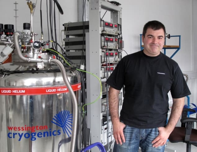
Nobel laureate Kostya Novoselov from the University of Manchester talks to Anna Demming about moving on from graphene and going back into 3D materials

When you and fellow Nobel laureate Andre Geim conducted the first experiments on isolated graphene in 2004 did you expect it would have so much impact?
No – definitely not. We were quite excited and understood it was something worth investigating, but because at the time we were outside the carbon research community we could not imagine what a wave of interest it would launch. It was very exciting for us and we could never have predicted it.
Did you foresee that there would be so many other interesting 2D materials to investigate?
That we realized pretty fast. The first paper on graphene was 2004 and the next year we published a paper on 2D atomic crystals in which we noted that graphene is not alone and there are actually many other interesting 2D materials (Proc. Natl. Acad. Sci 102 10451). Yet that paper was largely ignored for about five years because people were so fascinated with the unique properties of graphene. It was only afterwards that they came back to the other materials mentioned in the paper.
What is the current focus of your research?
Most of my research now is in heterostructures – 2D materials that are sandwiched together. Researchers have known about heterostructures for decades and a lot of good things have come from them. For example, many lasers and transistors are based on heterostructures of materials such as gallium nitride.
What is so interesting about them?
The range of opportunities. As it is possible to encapsulate unstable materials within the heterostructure “sandwich”, the breadth of materials available for study is greatly increased. Yet what is perhaps more interesting is that you can create devices and structures that cannot be made in any other way. For example, bringing conductive layers closer together than might otherwise be possible by separating them with an insulator layer. You can also do tunnelling experiments through very thin insulators or study magnetic barriers in tunnelling structures. There are many new experiments that become possible once you start creating these heterostructures.
Are these experiments motivated by fundamental science or applications?
Heterostructures allow you to go in both directions. You can explore the fundamental behaviour of structures and devices and interrogate the materials more thoroughly by subjecting them to a certain interaction. For example, because we can control the spacing on the atomic scale you can bring certain crystals together so that they start to interact, and then study this interaction. On the other hand, you can also create functional devices with heterostructures such as light-emitting diodes and photodetectors.
Discovery of ‘magic-angle graphene’ that behaves like a high-temperature superconductor is Physics World 2018 Breakthrough of the Year
Are these heterostructures challenging to make?
That’s one of the complexities – you need to create clean interfaces and keep them clean as you assemble the structures. As you get better at fabricating high-quality heterostructures, you start to see new phenomena appear. One example is that the properties of the heterostructures depend not just on what materials you stack together but also how you stack them. For instance, if you twist them they start to show different properties. So the more control we gain in the fabrication of heterostructures, the more interesting phenomena we can see.
Do you see the effects of twisted heterostructures playing a key role in the future?
Twisting is one of the “knobs” to control the behaviour of heterostructures. But I am sure there are many more. You can strain 2D crystals, you can fold them and so on – so there are more opportunities.
What particular heterostructure features have you found interesting?
We work on various tunnelling heterostructures, heterostructures involving magnetic materials, and identify the tunnelling properties of these devices by the twisting angle. Tunnelling is one of the ways to investigate one-atom-thick magnetic materials, but for us it is currently a playground rather than a way to an application.
Taking graphene from wonder material to real-world technologies
What heterostructure properties have the most potential for industry?
Several new types of devices have already been developed based on heterostructures. As to when they might start to make an appearance in industry, that’s a good question. Although we are reasonably proficient at making these devices in the lab, it will take some time before they can be created and mass produced by industry. But then again, 15 years ago no-one would have ever dreamed we would have mass-produced graphene, and now it is a routine operation.
What is the main challenge in translating these devices from the lab to industry?
We don’t have a definite method for how to make them – you can either grow these heterostructures or try to stack them together and it’s not clear which is the best method for industry. Just like graphene, there may be different types of applications, so the way to produce them may depend on that. I can imagine heterostructures being good for catalytic applications where you might have to grow them bottom up. Whereas for electronic applications you would try to produce them top down — preparing 2D crystals and then try to stack them together. What you need for industrial applications is some low-hanging fruit where the technology can be purified and polished, but I‘m not sure if we’ve got that at the moment.
Where do you see yourself working in the next 10 years?
I’m not an advocate for graphene or 2D materials. I’m doing this because the science is exciting. It’s good to see that developments in this area are turning into applications, but even if they didn’t, I would still be working on it because I find it interesting. But if something other than 2D materials becomes equally interesting I’ll do that instead.


