Bringing measurements across time, space and spectrum together is revealing the hidden dynamics of innovative optoelectronic devices and novel semiconductor materials
When evaluating new materials for optoelectronic applications – perhaps promising solar panel materials like halide perovskites or semiconductor compounds for microLED displays – optical characterization is almost always the materials scientists’ first port of call. And up to now steady-state photoluminescence (PL) has been the de facto workhorse for this task.
This non-destructive and highly sensitive technique involves optically exciting a sample and recording the integrated intensity and wavelength of re-emitted photons. Through this, researchers gain a quick understanding into a material’s electronic structure, optical transitions and emission characteristics.
However, these spectra alone can be misleading. Materials with substantially different microscopic properties can generate similar steady-state PL results, masking the fundamental physical dynamics that govern the material’s performance in the real world. To gain deeper understanding of a given material, a more comprehensive and correlated approach is needed.
Blinding average
The core issue lies in the fact that steady-state PL provides a time-integrated view of the emission and depending on the measurement geometry, may also average over spatial variations. Steady-state PL records a static equilibrium in which charge carrier generation balances recombination. This means that, on its own, it does not directly reveal how these excited charge-carriers evolve and ultimately dictate how a device manipulates energy and light.
For example, although two semiconductor thin films may show identical steady-state emission, they can perform very differently in a real device. One film might have long carrier lifetimes consistent with low non-radiative losses – useful in solar cells, for example – while the other could suffer from high defect densities that are masked by strong light absorption or intense excitation light.
Conversely, weak emission does not necessarily mean poor material quality. Again using a layered solar cell as an example, dim luminescence often signals fast, beneficial charge extraction across an interface rather than harmful defect recombination (where structural imperfections convert charge-carrier energy into wasted heat). Because steady-state measurements only show an overall average, they cannot separate these competing mechanisms.
Resolving in time, space and spectrum
Time-resolved PL (TRPL) is a key technique in illuminating these hidden dynamics. Unlike steady-state PL, which continuously bathes a sample with light, TRPL uses a short laser pulse and measures how the photoluminescence intensity evolves afterwards. This can reveal carrier dynamics over timescales ranging from picoseconds to microseconds.
TRPL is particularly important in materials where local variations strongly influence device behaviour. For instance, it can expose the difference between regions that exhibit long-lived emission consistent with efficient radiative recombination, and those that exhibit fast decay caused by, for example, defect recombination.
Of course, steady-state PL averages over time and space, and therefore TRPL only solves part of the problem. Spatially resolved TRPL addresses the missing spatial dimension. Combining a high-precision, motorized XY stage with TRPL’s precise timing, spatially resolved TRPL forms a 2D map that directly correlates localized structural features – such as grain boundaries and defects – with variations in carrier kinetics across the surface.
Complementary to these techniques is time-resolved emission spectroscopy (TRES), which combines spectral selection with time-resolved detection to measure how emission dynamics vary across the spectrum. By recording wavelength-dependent decay behaviour, TRES reveals how different spectral contributions evolve following excitation.
In short, where TRPL reveals kinetics over time and spatially resolved TRPL locates variations in space, TRES adds a spectral dimension, showing how the emission spectrum evolves after excitation. This allows researchers to track changes in the distribution of photon energies over time to understand carrier evolution and gain insight into the mechanisms underlying material behaviour.
A correlative approach
Though powerful in isolation, reconciling insights across these different instruments is slow and prone to errors. There can be microscopic differences between samples or even within positions in a single sample that dramatically alter emission spectra. Moreover, moving a sample between separate instruments is fraught with difficulty, potentially damaging the sample or causing delays that lead to sample degradation.
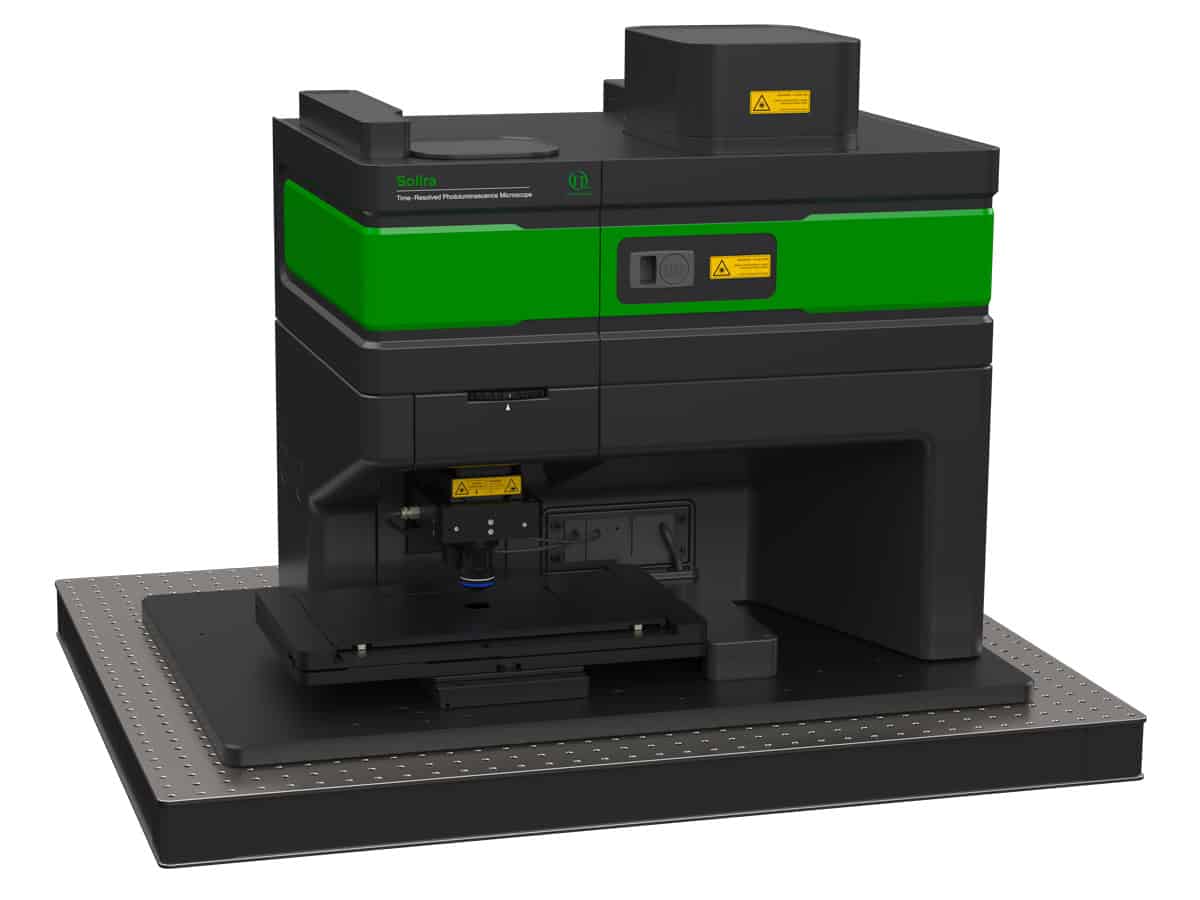
More comprehensive and reliable physical insight comes when temporal, spatial and spectral factors are recorded correlatively on the exact same sample region. This need for correlation is the motivation behind PicoQuant’s Solira, an integrated workflow platform for steady-state PL, TRPL, spatially resolved TRPL and TRES (the latter when combined with the complementary FlexLambda Kit), as well as additional imaging techniques, such as hyperspectral imaging, required for different scientific questions.
Bringing these techniques together within one configurable microscope system means a materials scientist can gain a more informed interpretation of material behaviour. For instance, they can identify the relevant emission bands at selected points of interest with steady-state PL. They can then wield TRPL to measure the associated decay kinetics, before perhaps applying TRES to resolve how those kinetics vary across the emission spectrum.
Bright demonstration
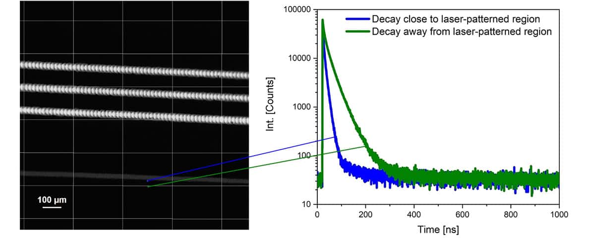
The power of this correlated approach was demonstrated recently by Professor Eva Unger’s group at Helmholtz-Zentrum Berlin, Germany, with measurements carried out by Maxim Simmonds. Investigating perovskite solar mini-modules, the team worked with PicoQuant and used Solira to locate precise laser-patterned lines – microscopic scribes used to interconnect individual cells in a solar module – before verifying emission from the active layer. Localized TRPL measurements then revealed significantly faster decay dynamics next to these laser cuts compared to the pristine bulk material, indicating altered carrier recombination or diffusion near structured features.
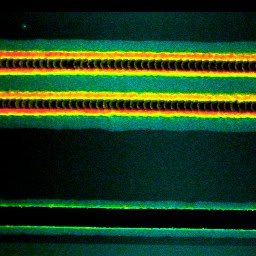
However, point measurements alone were not enough to discern whether the laser had fully removed the perovskite or merely modified it. Switching to spatially resolved TRPL imaging on Solira revealed that measurable photoluminescence persisted along the laser-patterned lines. This showed that laser structuring had altered local photophysical properties rather than eliminating the active layer – a conclusion only made possible by consistently mapping charge-carrier dynamics across temporal, spatial and spectral dimensions together on one setup.
As semiconductor materials and optoelectronic devices become more complex, optical characterization tools must keep pace. By unifying these tools within an integrated workflow platform such as Solira, materials scientists now have the means to paint a more complete picture of material characteristics and thereby unlock the next generation of innovative functional materials.