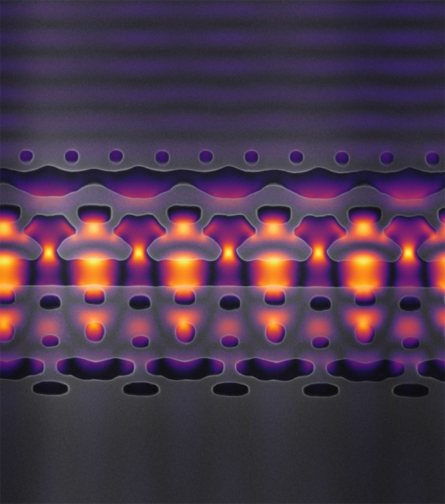
A laser-driven electron accelerator that is integrated on a chip has been created by Jelena Vučković and colleagues at Stanford University. The device was developed using inverse design algorithms and comprises a highly complex silicon waveguide that is driven by near-infrared pulses. Soon, the researchers hope that the technology can be used to accelerate electrons to energies of about 1 MeV.
Conventional accelerators use radio-frequency (RF) radiation to boost charge particles to relativistic speeds. While incredibly useful in both science and medicine, such accelerators are large and expensive – putting them out of reach of many universities, research institutes and hospitals.
Dielectric laser accelerators (DLAs) offer a promising way of creating smaller and cheaper electron accelerators. They work by firing pulses of visible or near-infrared light onto nanostructures such as silicon pillars or gratings. The nanostructures are in an evacuated channel through which a beam of low-energy electrons is sent to be accelerated by the light. By using radiation at much shorter wavelengths, DLAs can be around 10,000 times smaller than conventional RF accelerators.
Design challenges
However, DLAs also require bulky optical setups and this limits their scalability and robustness. Vučković’s team has shown that this problem can be overcome by using a photonic waveguide, which would enable DLAs to be integrated with compact photonic circuits. The challenge for the team was how to design a waveguide that is not degraded by scattering and reflection processes – something that was proving far too complex for a human to design.
The team addressed this issue by creating an “inverse design” algorithm, through which they could simply specify how much light energy they want to be delivered to electrons. From this input, the software calculates the precise silicon structure needed to deliver photon pulses to an incoming electron beam at just the right times and angles.
Metamaterial boosts performance of wakefield accelerator
The bizarrely-shaped prototype waveguide suggested by the algorithm was manufactured on a silicon-on-insulator chip using electron-beam lithography. The accelerating nanostructure was also created using inverse design. When the device is operated, pulses of light interact with electron pulses, boosting the kinetic energy of the electrons by 1.21 keV over a distance of just 30 microns.
As a fully integrated photonic circuit, the researchers’ DLA is highly robust and scalable. Vučković and colleagues now hope that these characteristics will enable them to use around 1000 accelerator stages to reach energies of 1 MeV – around 94% the speed of light – by the end of 2020.
One use of the technology that the team is working on is to channel electrons from the accelerator through an evacuated catheter and into the body. This would allow radiation to be delivered directly to tumours while minimizing radiation damage to healthy parts of the body.
The research is described in Science.


