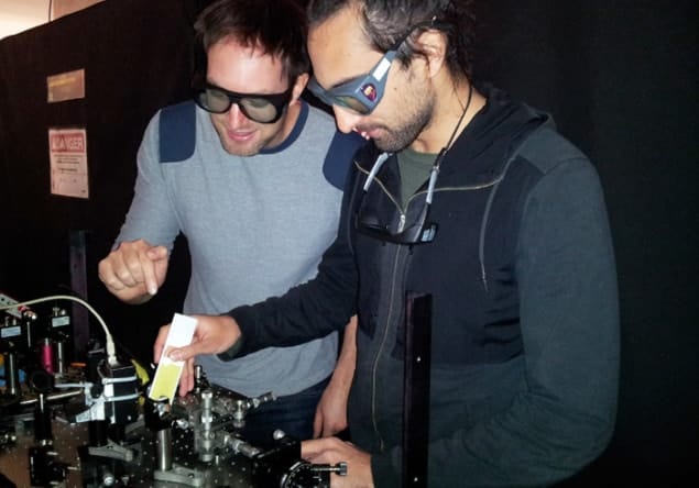
A new technique for measuring the electronic band structure of solid materials has been unveiled by physicists in Canada. The new method does not require the sample to be placed in a vacuum chamber and can also probe the bulk of a sample – something that some other techniques cannot do. The team believes that its new method could be particularly useful for studying matter under extreme conditions, including samples under extremely high pressure in a diamond anvil.
Angle-resolved photoemission spectroscopy (ARPES) is an important laser-based method for studying the electronic band structure of solid materials. Photons with enough energy to eject electrons from a material are fired at a sample and the energy and momenta of the emitted electrons are then measured. This information reveals the structure of the electronic bands in terms of the energy and momentum of the electrons within them.
Surface science
ARPES has been used extensively by physicists to study a wide range of materials including semiconductors and superconductors – but the technique has some important limitations. Measurements must be done in an ultra-high vacuum (UHV) because the emitted electrons are scattered and absorbed by air. Also, ARPES only probes a thin layer of material near the surface of the sample because the electrons cannot escape from deeper in the bulk.
Now, Paul Corkum and colleagues at the University of Ottawa, the Institut National de la Recherche Scientifique and the National Research Council of Canada have developed a new all-optical technique for studying the band structure of solids that overcomes these problems.
The technique involves exposing a sample to intense pulses of laser light, but with a photon energy much lower than that required to eject an electron from the material. There is a very large electric field associated with such a pulse, which causes an electron to quantum-mechanically tunnel from the top of the valence band to the bottom of the conduction band, thus creating a hole in the conduction band. The electron and hole are then driven by the electric field to high momenta in opposite directions. The electric field itself oscillates, and when the field direction switches, the electron and hole both reverse direction and are reunited. At this point, the electron and hole recombine, giving off a photon that can escape the material and be detected. The energy of the photon is equal to the energy gap between the valence and conduction band at the point of recombination.
To measure the momentum of the electron at recombination, Corkum and colleagues fire a much dimmer pulse from a different-coloured laser light at the sample, at the same time as the intense pulse. By measuring the intensity of the emitted light as a function of the phase between the light in the two laser pulses, the team can work out the momentum of the electron that recombined to produce the emitted photon.
Chemical processes
The electron–hole recombination process occurs very quickly, and this combined with the use of very short laser pulses means that the technique could be used to study changes in band structure over very short timescales.
Corkum says that the technique could prove particularly useful for studying materials under great pressure in a diamond anvil, because diamond is transparent to the laser light used to make the measurements. The method could be used to look at how the band structure of a material changes during catalysis and other chemical processes that cannot be studied in UHV. The study of materials in very high magnetic fields, which would deflect ARPES electrons, should also be possible.
The technique is described in Physical Review Letters.
