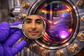
A two-dimensional semiconductor crystal just three atomic layers thick has emitted laser-like light. Crucially, this emission happened at room temperature: a significant improvement over previous cryogenic experiments. Coherent light generation from these ultrathin crystals paves the way for creating novel nanolasers, as well as opening doors for an emerging field of two-dimensional materials called valleytronics.
Exciton–polaritons
Researchers from the University of Oldenburg obtained coherent light from hybrid light–matter particles known as exciton–polaritons. These are formed from the strong interaction between confined photons and electrons. The process begins by exciting electrons in the two-dimensional crystal, which give off a photon. By placing the crystal between two optical mirrors, the photon can be reabsorbed, forming another excited electron. This electron–photon re-excitation process is then repeated, yielding a hybrid exciton–polariton.
Above a critical threshold emission, the exciton–polaritons transit into a macroscopic bosonic quantum state that generates spatially and temporally coherent light. Unlike normal laser light, it does not rely on population inversion, therefore requiring much lower lasing thresholds.
A class of semiconductors consisting of a transition metal and either sulphur, selenium or tellurium is known to possess a strong interaction with light. In this case, the team used a single layer of tungsten diselenide (WSe2) crystal to strongly couple to light. Their previous experiments used a slightly different crystal (molybdenum diselenide) at cryogenic temperatures, but the researchers were now ready to make the step into warmer territory. They publish their latest findings in Nature Communications.
And then there was light
Electrons within the material were kicked into action with a green laser that was progressively increased in power to reach the lasing threshold. Exciton–polaritons were created in a trap (a few micron-sized WSe2 monolayer), and light was captured between two distributed Bragg reflectors (DBRs) that act as mirrors.
The team then tested the spatial coherence of the light using a Michelson interferometer and noticed a very small coherence length before the threshold value, followed by a significant increase after the threshold. Additionally, the emitted light showed high temporal coherence. Such high temporal and spatial coherence are key signatures of exciton–polariton lasing.
Magnets reveal the smoking gun
When placing the sample inside a magnetic field, the researchers observed a spectral Zeeman splitting: a phenomenon that occurs due to the electrons slightly changing orbits. The applied magnetic field induced the energy splitting of the polariton emission into two circularly polarized light components, which are linked to the local extrema in the electronic band structure in the semiconductor material, called valleys, in which the two-dimensional excitons are formed. Since photons do not respond to a magnetic field, this magnetic Zeeman splitting was another tell-tale sign of exciton–polariton emission.
Carlos Antón-Solanas and Christian Schneider, leaders of this research work, explain that spatial coherence had been associated with a “smoking gun criterium” years ago. “But our work is the first to report these central results,” Antón-Solanas adds. He explains that the step to room temperature was made possible by changing to WSe2: a material where the exciton photoluminescence can be reached at elevated temperatures, and exciton–polaritons present a sufficiently long lifetime enabling their formation before decay.
Antón-Solanas notes that another group published monolayer emission results around the same time as they, albeit with a different material (tungsten disulphide) that emits at a different wavelength.
New fields
On future steps, Schneider says that the team will study the photon-number composition of the lasing polariton emission via second-order correlations experiments, as well as signatures of superfluidity and superconductivity. As for applications, Schneider thinks that the polariton lasing can be applied to micro- and nano-devices. The control over the polarization and energy structure of the polaritons also looks promising for applications in nanophotonic valleytronic devices: an emerging field in which the valleys inside semiconductor material are used to store, manipulate and read out bits of information.
Exotic quantum state could make smallest-ever laser
Ritesh Agarwal from the University of Pennsylvania, who was not involved in this research, thinks that these studies are important as they show macroscopic coherence of matter at room temperature in relatively “unclean” materials that don’t require the highly advanced optical cavity designs seen in traditional optical materials.
Agarwal adds that their rather simple fabrication procedures will make these systems more accessible to many researchers, leading to many more discoveries of new and intriguing phenomena. “This study, which adds to a rapidly growing body of work, is in the right direction to fabricate novel polaritonic devices for photonics applications,” he concludes.


