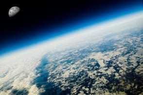
For many, images from outer space are wonder pictorialized, glimpses of the primordial past made possible with the technology of the future. In reality the need to mitigate risks to multibillion dollar space missions can dampen the haste to adopt new technologies. But old tools cannot always deliver new tricks, and efforts to develop new equipment and methodologies to achieve the unprecedented measurements in unchartered extraterrestrial territory continue to attract considerable investment. Nanomaterials punch way above their weight in terms of functionality. Physics World looks at whether this is enough to earn their place in space.

For aerospace every kilo has to count. Meyya Meyyappan, chief scientist for exploration technology at Ames Research Center, put the cost of every kilogram launched into near-Earth orbit at close to USD$25,000. Aim for further afield and that figure increases by a factor of 10. The instrumentation demands that need to be met within these requirements are extreme – both to control and maintain the space craft, as well as monitoring the health of any humans who may be on board. Above and beyond the basic subsistence of the craft and crew, there is the raison d’etre of the mission – taking unprecedented measurements with an accuracy and reliability such that the results add to the sum total of human knowledge in a way that justifies the cost of the mission in the first place. No small wonder then that space missions continue to invest in new technologies.
Looking into space
An exciting aspect of detecting photons in space missions is the view it gives not just into distant space but into the distant past, as photons from the far extremes of the Universe take vast periods of time to reach us. Capturing these photons requires detectors for vanishingly low photon intensities. Superconducting nanowires have been a popular option to explore here as they are very sensitive to photons, which break up the Cooper pairs. This way superconducting nanowires can detect intensities as low as single photons. Although superconducting devices have strict cooling requirements Robert Hadfield at the University of Glasgow and colleagues in STFC Rutherford Appleton Laboratory in the UK, Single Quantum BV in the Netherlands and KTH Royal Institute of Technology in Sweden have already miniaturized a platform for superconducting photon detectors that operate at 4 K, and seen it launched aboard the Ariane 5 rocket in 2009 as part of the Planck mission.
Can nanomaterials take on the extremes of space?

The snag with superconductor photon detectors has been that the sensitivity rapidly diminishes as the photon energy decreases, limiting their range within the electromagnetic spectrum. To tackle this a team led by Dirk Englund at MIT developed a device based on graphene contacted at both ends by a superconducting material. The device – a form of Josephson junction – can sustain a superconducting current unless incident photons heat up the graphene and break up the Cooper pairs. Importantly this device is more sensitive to lower-frequency photons. “First, graphene can absorb light at nearly any wavelength in the electromagnetic spectrum. Second, because graphene is two-dimensional, it can be easily integrated into structures that can further enhance its light absorption,” said Englund. This view of low-energy radiation provides observations of some of the faintest objects in the universe.
It turns out graphene also comes in handy at higher energies. Radiation in the 10-200nm range can give information on solar storms and the way nebulae expand, but current technology to detect in this range – violet chromatographs and microchannel plates – are not just heavy, whacking up payload costs, but they are power hungry too. Photovoltaic devices that require zero power are the ideal alternative, and reports from China of a heterojunction device based on p-type graphene could represent a breakthrough for this type of detector. “The new VUV-light-detecting device, being much lighter than existing detectors, could also help lower launch costs of the spacecraft carrying it,” said Feng Huang of the School of Materials at Sun Yat-Sen University in Guangzhou.
While great progress has been made in the sensitivity of superconducting radiation detectors, according to researchers at the University of Jyväskylä the next goal is increasing the number of detector pixels in single devices, which has so far been limited by device heating. Having stumbled upon the giant thermoelectric effect, these researchers are now leading the SUPERTED consortium to use the phenomenon to solve heat issues in radiation detection. “The idea is old, but the problem has been to find a strong enough thermoelectric effect,” says consortium leader Tero Heikkilä from the University of Jyväskylä department of physics. “We found it in 2014 by accident as we were studying the properties of hybrid structures of superconductors and magnets. Our theoretical prediction was experimentally demonstrated in 2016.” The consortium has attracted support from the European Commission who are investing 3 million euros of funding to develop ultrasensitive sensors of electromagnetic radiation based on hybrid structures of superconductors and magnets.
Sniffing into space
Probing for biological and chemical data from space, as well as monitoring the crew, their food and their environment, requires chemical and biosensors that are ideally small, light, specific, robust to different environments and energy efficient. A lot of current sensors are power hungry and have high environmental requirements, such as operating temperatures of 200 °C, taking the widely used tin oxide thin film sensors as an example. As a result, there has been a lot of research into exploiting nanomaterials instead, with their high surface area to volume ratio and the sensitivity of their properties to chemical and biological analytes.
The potential of carbon nanotubes for sensing applications has long attracted notice. Carbon nanotubes have shown potential for sensing a wide range of substances including glucose, an important indicator of metabolic health. As far back as 2013 AT Charlie Johnson and colleagues were able to demonstrate sensitivity to glucose at concentrations as low as 1 μM by functionalizing the nanotubes with highly negatively charged pyrene boronic acid. “These low concentrations fall within the range at which glucose is found in saliva,” said Johnson. CNTs can also detect harmful gases in the atmosphere with simple devices distinguishing between carbon monoxide and carbon dioxide based on how readily the molecules adhere to the nanotubes.
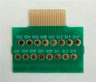
Taking advantage of the wide range of analytes CNT sensors can detect, Meyya Meyyappan and colleagues have combined 16 CNT sensors onto a chip. “In addition to purified SWCNTs, variations in sensor material may include doping, metal loading, coating or functionalization of the nanotubes and the use of metal oxide nanowires or nanoparticles, to elicit a signal from the analyte of interest, as pure SWCNTs might not respond to every gas or vapor,” they explain in a report referring to the work. They then train the devices in the lab to distinguish different gases based on the effect on the resistance of each sensor and as a result the pattern of resistance on the chip, thereby producing an “electronic nose”.
Nanotechnology launch off
The key characterization tools that first brought nanostructures into view were the scanning tunnelling microscope for conducting samples and the atomic force microscope developed shortly afterwards for imaging non-conducting samples. Thirty years on these tools remain crucial analysis tools for nanostructure characterization both on and off planet Earth.
When the Rosetta orbiter launched in 2014 it carried a micro-imaging dust analysis system (MIDAS) featuring an atomic force microscope. As the orbiter trailed after comet 67P/Churyumov-Gerasimenko it was able to collect data on the structure of dust samples from the comet with the aid of MIDAS. Comparing the structure with the predictions of planetary accretion models has helped to gain insights into likely scenarios as to how the solar system formed, providing another glimpse back in time.
Despite the restrictive payload costs, not just nanomaterials but their characterization devices have already made it onto space missions. Given the fit of space mission requirements and what nanomaterials have to offer it seems reasonable to expect the role of nanomaterials in tooling up space missions to literally sky rocket.