Solar cells are a great alternative energy source – when the Sun is out. To reap the benefits of solar power at other times requires some means of energy storage, and a popular choice is splitting water into hydrogen and oxygen – “hydrogen storage”. Researchers at The Australian National University in Canberra have now fabricated an inverse opal structure uniformly coated in CdS as a photoanode for splitting water that outperforms all other reported CdS-based devices.
A compound as common as water is an appealing resource to exploit for alternative energy storage. But splitting water for hydrogen generation requires a semiconductor that can provide charge carriers with the right energy for both the reduction and oxidation reactions of hydrogen and oxygen, and here cadmium sulphide with its low photoconversion efficiency and high tendency to corrode is one of a very short list of candidates. While there are reports of successfully preventing corrosion using co-catalysts in heterostructure configurations with TiO2 and ZnO nanostructures, these heterostructures remain prone to poor control over thickness and uniformity in high aspect-ratio forms.
“Photoelectrochemical generation of hydrogen from water using a semiconductor material involves various important steps including electron-hole pair generation, charge separation, transfer and surface chemical reactions,” explains Siva Karuturi, the lead author on the report of these results. “These processes are highly sensitive to the semiconductor film properties such as uniformity of its distribution in nanostructured surfaces. Thus, achieving uniformity control plays a prominent role in improving the overall photoelectrochemical performance.”
Karuturi and his colleagues, led by Chennupati Jagadish, achieved this uniformity by combining atomic layer deposition (ALD) and solution ion transfer (SIT) to coat TiO2 inverse opals in CdS. “To our understanding, this is the first report of CdS from the SIT method, although various chemical and physical methods of synthesizing CdS have been reported previously including SILAR,” says Karuturi. “Most of the reported methods fail to achieve conformal CdS coating with uniform distribution in a high aspect ratio nanostructure. The SIT method solves this long-standing issue and it can be extended to many semiconductors.”
The resulting structures achieved a saturation photocurrent density of 9.1 mA cm−2 – the highest ever reported for CdS-based photoelectrodes – and paves the way for unassisted solar hydrogen generation.
The precise advantages of ALD with SIT
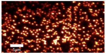
The researchers created an inverse opal structure of TiO2 by coating polystyrene beads using ALD, a process that exposes the structure to the constituent elements of the desired chemical to build up a coating of one atomic layer at a time. The process is particularly useful for creating uniform, high-quality coatings with excellent thickness control. Subsequent heat treatment removed the beads leaving the TiO2 inverse opal – a structure with many advantages for catalysis.
“Inverse opal is a three-dimensional interconnected nanostructure offering high interfacial surface, which is critical for efficient catalytic reactions and direct charge transport paths,” explains Karuturi. “Besides, its feature size is comparable to the wavelength of incident light providing opportunities to tailor light–matter interactions.”
While direct deposition of CdS with ALD can be an option to achieve uniform CdS coating on high aspect ratio surfaces, ALD metal sulfide processing is shown to be complex and requires handling of toxic substances in gaseous form. Instead the researchers used the same ALD process to coat the TiO2 inverse opal structure with 10 nm of ZnO, before subsequent anion and cation exchange SIT steps to convert the ZnO film first into ZnS and then CdS, respectively.
Adding a further 1.5 nm of amorphous TiO2 helped improve the photoconversion efficiency further by suppressing carrier recombination. The researchers attribute the record saturation photocurrent density of ∼9.0 mA cm−2 and hydrogen gas generation rate of 141.3 μmol cm−2 h−1 at 0.1 V versus RHE to the improved interfacial charge transfer and high quantum efficiency. They also report a photocurrent density of 6.6 mA cm−2 at 0 V versus RHE, which suggests the potential of the structure for unassisted solar hydrogen generation.
Next steps
Previous work has attempted hydrogen solar energy storage by water splitting using either a dual-electrode cell configuration – one for the oxidation and another for the reduction steps – or combining separate photovoltaic light harvesting and electrolytic water splitting systems. Demonstrating this improved photoconversion efficiency with a CdS-based system demonstrates the practical potential of an electrolytic cell based on a single bandgap semiconductor as a simpler and more cost-effective alternative.
The researchers are now working to improve the stability of CdS non-sacrificial electrolytes and the possible extension of this SIT fabrication approach to other semiconductor systems.
Full details are reported in Nano Futures.