When diamond defects emit light, how much of that light can be captured and used for quantum technology applications? According to researchers at the Hebrew University of Jerusalem, Israel and Humboldt Universität of Berlin, Germany, the answer is “nearly all of it”. Their technique, which relies on positioning a nanoscale diamond at an optimal location within a chip-integrated nanoantenna, could lead to improvements in quantum communication and quantum sensing.
Nitrogen-vacancy (NV) centres are point defects that occur when one carbon atom in diamond’s lattice structure is replaced by a nitrogen atom next to an empty lattice site (a vacancy). Together, this nitrogen atom and its adjacent vacancy behave like a negatively charged entity with an intrinsic quantum spin.
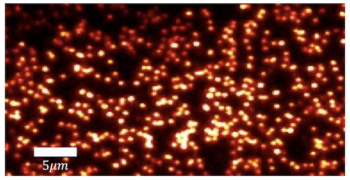
When excited with laser light, an electron in an NV centre can be promoted into an excited state. As the electron decays back to the ground state, it emits light. The exact absorption-and-emission process is complicated by the fact that both the ground state and the excited state of the NV centre have three sublevels (spin triplet states). However, by exciting an individual NV centre repeatedly and collecting the photons it emits, it is possible to determine the spin state of the centre.
The problem, explains Boaz Lubotzky, who co-led this research effort together with his colleague Ronen Rapaport, is that NV centres radiate over a wide range of angles. Hence, without an efficient collection interface, much of the light they emit is lost.
Standard optics capture around 80% of the light
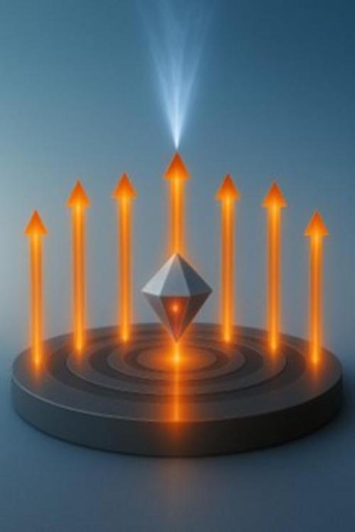
Lubotzky and colleagues say they have now solved this problem thanks to a hybrid nanostructure made from a PMMA dielectric layer above a silver grating. This grating is arranged in a precise bullseye pattern that accurately guides light in a well-defined direction thanks to constructive interference. Using a nanometre-accurate positioning technique, the researchers placed the nanodiamond containing the NV centres exactly at the optimal location for light collection: right at the centre of the bullseye.
For standard optics with a numerical aperture (NA) of about 0.5, the team found that the system captures around 80% of the light emitted from the NV centres. When NA >0.7, this value exceeds 90%, while for NA > 0.8, Lubotzky says it approaches unity.
“The device provides a chip-based, room-temperature interface that makes NV emission far more directional, so a larger fraction of photons can be captured by standard lenses or coupled into fibres and photonic chips,” he tells Physics World. “Collecting more photons translates into faster measurements, higher sensitivity and lower power, thereby turning NV centres into compact precision sensors and also into brighter, easier-to-use single-photon sources for secure quantum communication.”
Nanodiamond quantum thermometer measures the temperature of worms

The researchers say their next priority is to transition their prototype into a plug-and-play, room-temperature module – one that is fully packaged and directly coupled to fibres or photonic chips – with wafer-level deterministic placement for arrays. “In parallel, we will be leveraging the enhanced collection for NV-based magnetometry, aiming for faster, lower-power measurements with improved readout fidelity,” says Lubotzky. “This is important because it will allow us to avoid repeated averaging and enable fast, reliable operation in quantum sensors and processors.”
They detail their present work in APL Quantum.